.png?width=50&height=50&name=mcc%20150x150%20(1).png)
Ultra‑Miniature SOT‑563 Package for High‑Density Switching and Level Shifting
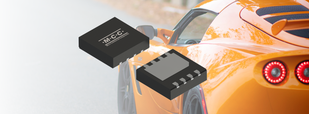
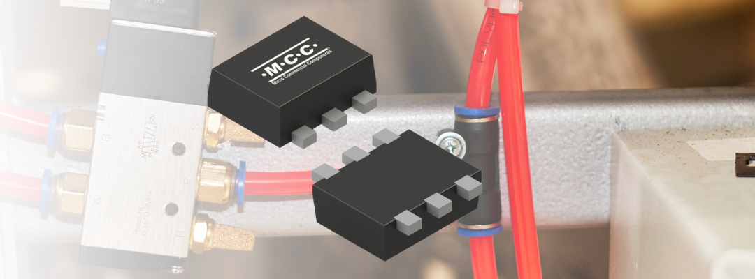
MCC launches the BSS138KV, a compact 60V dual N‑channel MOSFET designed for modern electronics that demand more functionality in less space without compromising efficiency or reliability. This device integrates two independent 60V N‑channel MOSFETs with ESD protection into an ultra‑miniature SOT‑563 package.The space‑saving design significantly reduces component count and PCB footprint, making it ideal for portable, battery‑powered, and high‑density applications.
Built on advanced trench LV MOSFET technology, the BSS138KV‑TP delivers low Rds(on) and low threshold voltage, minimizing conduction and switching losses for improved system efficiency even at low gate drive levels. Its dual configuration simplifies load switching, level shifting, and signal routing, enabling designers to optimize circuit architecture across multiple voltage domains.
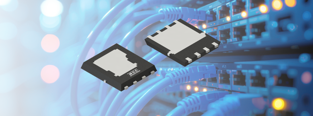
With integrated ESD‑protected gates and robust process technology, the device ensures long‑term reliability in harsh or noise‑prone environments. From consumer electronics and IoT devices to industrial automation and wearables, the BSS138KV‑TP offers a compact, efficient, and flexible solution for today’s space‑constrained designs.

Features & Benefits:
- 60V dual N‑channel MOSFET in ultra‑miniature SOT‑563 package
- Very small footprint SOT‑563 package: approximately 1.6 mm × 1.6 mm body size
- Trench LV MOSFET technology optimized for low switching losses and higher efficiency
- Low threshold voltage suitable for low gate drive operation
- Low Rds(on) for reduced conduction losses and improved system efficiency
- Integrated ESD‑protected gate for enhanced robustness and long‑term reliability
- Dual independent N‑channel configuration for flexible load/power switch topologies
- Ideal for high‑density, space‑constrained PCB layouts and portable devices
Applications
|
|
|
|
|
|
Consumer Electronics & Computing |
Industrial, Automation & Instrumentation |
IoT, Smart Home & Connected Devices |
Communications & RF Interfaces |
|
|
|
|


Product Attributes, Parametrics & Datasheet
|
Product |
Type |
Package |
Number of Functions |
Channel |
Drain-Source |
Gate-Source |
RDS(ON) |
Datasheet |
|
Small Signal MOSFET |
Dual |
N+N |
60 |
±20 |
3.3 |
Now available, purchase directly from MCC or through our authorized distributors.
MCC MOSFETs deliver reliable switching, low on-resistance, and compact footprints for industrial and automotive applications, including AEC-Q101 qualified options and efficient packages across diverse power ranges. Learn more in The Essential Guide to 40V MOSFET Functions & Features or explore our full portfolio Small Signal MOSFET Products.
For technical inquiries or sample requests, contact MCC for support.
%20(3).png)