---
title: "Application Note: Quick Guide on Automotive Load Dump Protection (ISO 16750-2)"
description: At Micro Commercial Components (MCC), we are committed to transparency, reliability, and continuous improvement for our global customers.
image: https://solutions.mccsemi.com/hubfs/MCC_strenghten_its_future.png
---
###### Utility Navigation
- [ 0](https://cart.mccsemi.com/cart)
- [Login / Sign Up](https://www.mccsemi.com/Identity/Account/Login)
- [Terms of Sale and Export](https://www.mccsemi.com/Home/TermsAndConditions)
- [中文](https://www.mccsemi.com/Home/SetLanguage?returnUrl=%2FContact)
[ ](https://www.mccsemi.com/)
###### Main Navigation
- [Products](https://www.mccsemi.com/ProductCategories)
#### Products
MCC produces high-quality discrete semiconductors to the consumer and industrial markets—including diodes, rectifiers, MOSFETs, voltage regulators and protection devices.
[View Products](https://www.mccsemi.com/ProductCategories)
- **Diodes**
- [Zener Diodes](https://www.mccsemi.com/product/ZenerDiodes)
- [Switching Diodes](https://www.mccsemi.com/product/SwitchingDiodes)
- [Small Signal Schottky Diodes](https://www.mccsemi.com/product/SmallSignalSchottkyDiodes)
- [Bridge Rectifiers](https://www.mccsemi.com/product/BridgeRectifiers)
- [Standard Recovery Rectifiers](https://www.mccsemi.com/product/StandardRecoveryRectifiers)
- [Fast Recovery Rectifiers](https://www.mccsemi.com/product/FastRecoveryRectifiers)
- [Super Fast Recovery Rectifiers](https://www.mccsemi.com/product/SuperFastRecoveryRectifiers)
- [Schottky Barrier Rectifiers](https://www.mccsemi.com/product/SchottkyBarrierRectifiers)
- **MOSFETs**
- [Small Signal MOSFETS](https://www.mccsemi.com/product/SmallSignalMOSFETS)
- [Power MOSFETS](https://www.mccsemi.com/product/PowerMOSFETS)
- [Wide SOA MOSFETs](https://www.mccsemi.com/product/PowerMOSFETS)
- **Transistors**
- [Small Signal Bipolar Transistors](https://www.mccsemi.com/product/SmallSignalBipolarTransistors)
- [Medium Power Bipolar Transistors](https://www.mccsemi.com/product/MediumPowerBipolarTransistors)
- [Pre-biased Transistors](https://www.mccsemi.com/product/PreBiasedTransistors)
- [Darlington Transistors](https://www.mccsemi.com/product/PreBiasedTransistors)
- [**Voltage Regulators**](https://www.mccsemi.com/product/VoltageRegulators)
- [**Protection Devices**](https://www.mccsemi.com/product/TVs)
- [TVS](https://www.mccsemi.com/product/TVs)
- [ESD Protection](https://www.mccsemi.com/product/ESDProtectionDevices)
- Programmable Thyristor Surge Suppressor
- **Silicon Carbide (SIC)**
- [SiC Schottky Barrier Diodes (SBDs)](https://www.mccsemi.com/products/silicon-carbide-sic/sic-schottky-barrier-diodes-sbds)
- [SIC MOSFETS](https://www.mccsemi.com/product/SICMOSFETS)
- **IGBT**
- [IGBT Discrete](https://www.mccsemi.com/product/IGBTDiscrete)
- [IGBT Modules](https://www.mccsemi.com/product/IGBTModules)
- **Power Modules**
- [Standard Recovery Power Modules](https://www.mccsemi.com/product/StandardRecoveryPowerModules)
- [Thyristor Modules](https://www.mccsemi.com/product/ThyristorModules)
- [Fast Recovery Modules](https://www.mccsemi.com/product/FastRecoveryModules)
- [Schottky Modules](https://www.mccsemi.com/product/SchottkyModules)
#### [ Product Offerings](https://www.mccsemi.com/ProductCategories)
- [Applications](https://www.mccsemi.com/applications)
#### Applications
MCC offers a broad range of solutions with ready to go design solutions in various segments such as Automotive, Industrial, Computing & Personal Electronics and Consumer. Please contact our sales team or distributors to get samples or more information..
[View Application Overview](https://www.mccsemi.com/applications)
- [**Automotive**](https://www.mccsemi.com/applications/automotive)
- [Front & Rear LED Lights](https://www.mccsemi.com/applications/automotive/front-rear-led-lights-or-exterior-led-lights)
- [LED backlights (touch screen, cameras)](https://www.mccsemi.com/applications/automotive/led-backlights-touch-screen-cameras)
- [Electric Power Steering (EPS)](https://www.mccsemi.com/applications/automotive/electric-power-steering-eps)
- [Automotive Interior LED Lighting](https://www.mccsemi.com/applications/automotive/automotive-interior-led-lighting)
- [Infotainment in Cabin](https://www.mccsemi.com/applications/automotive/infotainment-in-cabin)
- [Battery Management System (BMS) for EVs](https://www.mccsemi.com/applications/automotive/battery-management-system-bms-for-evs)
- [Auto Seat Controls](https://www.mccsemi.com/applications/automotive/auto-seat-controls)
- [Instrument Cluster](https://www.mccsemi.com/applications/automotive/instrument-cluster)
- [Body Control Module (BCM)](https://www.mccsemi.com/applications/automotive/body-control-module-bcm)
- [Advanced Driver Assistance System (ADAS) Sensor Module](https://www.mccsemi.com/applications/automotive/advanced-driver-assistance-system-adas-sensor)
- [Fast EV Charger](https://www.mccsemi.com/applications/automotive/fast-ev-charger)
- [**Computing & Personal Electronics**](https://www.mccsemi.com/applications/computing--personal-electronics)
- [Solid State Drive (SSD)](https://www.mccsemi.com/applications/computing--personal-electronics/solid-state-drive-ssd)
- [DC Fan](https://www.mccsemi.com/applications/computing--personal-electronics/dc-fan)
- [Uninterruptible Power Supply (UPS)](https://www.mccsemi.com/applications/computing--personal-electronics/uninterruptible-power-supply-ups)
- [Notebook Computer](https://www.mccsemi.com/applications/computing--personal-electronics/notebook-computer)
- [DC-DC Converters](https://www.mccsemi.com/applications/computing--personal-electronics/dc-dc-converters)
- [AC-DC Adaptor](https://www.mccsemi.com/applications/computing--personal-electronics/ac-dc-adaptor)
- [**Industrial**](https://www.mccsemi.com/applications/industrial)
- [AC-DC Power Supply Unit](https://www.mccsemi.com/applications/industrial/ac-dc-power-supply-unit)
- [Energy Storage Systems (ESS)](https://www.mccsemi.com/applications/industrial/energy-storage-systems-ess)
- [Smart Energy Meters](https://www.mccsemi.com/applications/industrial/smart-energy-meters)
- [Solar Inverters](https://www.mccsemi.com/applications/industrial/solar-inverters)
- [Electric Panel Switch for Solar System](https://www.mccsemi.com/applications/industrial/electric-panel-switch-for-solar-system)
- [**Consumer**](https://www.mccsemi.com/applications/consumer)
- [Smart Door Lock Systems](https://www.mccsemi.com/applications/consumer/smart-door-lock-systems)
- [Cordless Power Tool Motor Unit](https://www.mccsemi.com/applications/consumer/cordless-power-tool-motor-unit)
- [Cordless Power Tool Battery Charger](https://www.mccsemi.com/applications/consumer/cordless-power-tool-battery-charger)
- [Cordless Power Tool Battery Pack](https://www.mccsemi.com/applications/consumer/cordless-power-tool-battery-pack)
- [Smoke Detector](https://www.mccsemi.com/applications/consumer/smoke-detector)
- [Basic Class D amplifier](https://www.mccsemi.com/applications/consumer/basic-class-d-amplifier)
- [E-bike Battery Management System](https://www.mccsemi.com/applications/consumer/e-bike-battery-management-system)
- [Simple Flyback Topology LED](https://www.mccsemi.com/applications/consumer/simple-flyback-topology-led)
- Cordless Lawn Mower
#### [ Application](https://www.mccsemi.com/applications)
- [Knowledge Center](https://solutions.mccsemi.com/knowledge-center)
#### Knowledge Center
Expand your knowledge and optimize your designs with our robust library of tools, resources, and more.
[Learn More](https://solutions.mccsemi.com/knowledge-center)
- [**New Product Introductions**](https://solutions.mccsemi.com/news/tag/new-product-introductions)
- [News](https://solutions.mccsemi.com/news/tag/news)
- [Blog](https://solutions.mccsemi.com/news/tag/blog)
- [Guides](https://solutions.mccsemi.com/guides)
- [Webinars](https://solutions.mccsemi.com/news/tag/webinars)
- [Reference Boards](https://solutions.mccsemi.com/news/tag/reference-boards)
- [**Product Catalog**](https://www.mccsemi.com/pdf/MCCProductCatalog.pdf)
- [SMD Dimension Selection Guide](https://www.mccsemi.com/pdf/SMDDimensionSelectionGuide.pdf)
#### [ Knowledge Center](https://solutions.mccsemi.com/knowledge-center)
- [Quality](https://www.mccsemi.com/Quality)
#### Quality
Our commitment to manufacturing and delivering best in class quality components that meets the market and our customer expectations.
[Quality Overview](https://www.mccsemi.com/Quality)
- [**Quality Overview**](https://www.mccsemi.com/Quality)
- [ECN/PCN](https://www.mccsemi.com/ECNPCN/List)
- [IMDS Request Form](https://www.mccsemi.com/imds)
- [Environmental Program](https://www.mccsemi.com/Quality)
- [Certifications](https://www.mccsemi.com/Quality/Certifications)
- [Reliability Data](https://www.mccsemi.com/ReliabilityData)
- [MSL](https://www.mccsemi.com/pdf/MSL.pdf)
- [Return Policy: Failure Analysis](https://www.mccsemi.com/pdf/ReturnPolicy.pdf)
#### [ Quality Overview](https://www.mccsemi.com/Quality)
- [About](https://www.mccsemi.com/Home/CompanyProfile)
#### Company Profile
Our company has extensive experience in the manufacturing and delivery of high-quality components.
[View Company Profile](https://www.mccsemi.com/Home/CompanyProfile)
- [Company Profile](https://www.mccsemi.com/Home/CompanyProfile)
- [Meet the team](https://www.linkedin.com/company/micro-commercial-components-mcc-)
- [Careers](https://www.mccsemi.com/careers)
- [Events](https://www.mccsemi.com/events)
- [Contact Us](https://www.mccsemi.com/Contact/Index)
- History
#### [ Company Overview](https://www.mccsemi.com/Home/CompanyProfile)
- Support
#### Utility Resources
Additional MCC resources to assist in company, products, quality information, and supply chain alerts.
Utility Overview
- [Product Packaging](https://www.mccsemi.com/Package/List)
- [Component Weight Information](https://www.mccsemi.com/Package/List)
- [Supply Chain Alerts](https://development.mccsemi.com/supplychainalerts#pageNumber=0)
- [Longevity Program](https://www.mccsemi.com/pdf/LongevityProgram.pdf)
- [Package Outline (PDF)](https://www.mccsemi.com/pdf/PackageOutline.pdf)
#### Resources Overview
- [ 0](https://cart.mccsemi.com/cart)
- [Login / Sign up](https://www.mccsemi.com/Identity/Account/Login)
- [Terms & Conditions](https://www.mccsemi.com/Home/TermsAndConditions)
- [中文](https://www.mccsemi.com/Home/SetLanguage?returnUrl=%2FContact)
Toggle Main Navigation
Subscribe to our newsletter
Categories
×
### Subscribe to receive insights from MCC!
Sign up and never miss an update.
# Application Note: Quick Guide on Automotive Load Dump Protection (ISO 16750-2)
# Application Note: Quick Guide on Automotive Load Dump Protection (ISO 16750-2)
.png?width=50&height=50&name=mcc%20150x150%20(1).png)
by [MCC](https://solutions.mccsemi.com/news/author/mcc)
July 08, 2026
## Part 1: Understanding ISO 16750-2 Load Dump Pulses and TVS Diode Calculation for Automotive Protection
---
### **01**
### **Introduction**
Electric and non-electric vehicles have increasingly incorporated electronic features to enhance both performance and comfort. With recent technological advances, these devices, modules, and components have continued to shrink in size-a desirable characteristic that, however, can also make them more vulnerable to unexpected electrical surge events.
ISO 16750-2 describes in detail several types of electrical transients that can occur in automotive systems. Among the various defined pulses, this document focuses on the load dump event, designated as Test A and Test B (ISO 7637-2 names this pulse 5a and 5b, however these pulses were removed from the document to refer to ISO 16750-2 pulse definitions; it’s worth noting that is still a common practice in the industry to name load dump pulse as “Pulse 5”).
Load dump is characterized as a discontinuity in supply voltage condition caused by the unexpected disconnection of the battery from the supply circuit while the system is energized.
Among the available solutions for mitigating surge events, the transient voltage suppressor (TVS) diode is almost always present. Whether used as the primary protection element or as part of a multistage protection scheme, TVS diodes are considered essential in circuits operating at higher voltages. They provide an initial clamping action or supplementary protection in conjunction with other devices, limiting overvoltage stress on low voltage modules and secondary circuits.
In this application note, a practical methodology for automotive load dump protection is presented, focusing on the selection of a suitable TVS diode capable of withstanding ISO 16750-2 load dump transients. The guide explains the key parameters required for TVS diode selection, including reverse working voltage, clamping voltage, peak pulse current, and peak pulse power, and demonstrates how to evaluate compliance with ISO 16750-2 Test A and Test B conditions.
By applying these design principles, engineers can improve the robustness, reliability, and surge immunity of automotive electronics, including ECUs, DC-DC converters, power distribution modules, and other vehicle electronic systems exposed to high-energy load dump events.
---
### **02**
### **What Is Automotive Load Dump and How Does a Load Dump Event Damage Electronics?**
Load dump is a type of transient event that occurs in automotive electrical systems when the alternator is supplying current to charge the battery and the latter is abruptly disconnected, either by accidental disconnection, corroded terminals, poor connection or degraded cables.
This sudden abrupt loss of connection results in a rapid overvoltage transient that can damage multiple loads and electronic modules that remain connected to and powered by the alternator, as illustrated in Figure 1.
The key parameters required to characterize and protect systems against load dump events are the *Surge Voltage* *(Vp)* and the *Pulse Duration (td)*. The pulse amplitude depends primarily on the alternator speed and the level of field excitation when the battery is disconnected.
The pulse duration further contributes to the severity of the event, as it subjects electronic components to sustained overvoltage stress. Depending on the system voltage, the load dump pulse duration can range from approximately 350ms in 24V systems to up to 400ms in 12V systems, significantly challenging the power handling capability of protection devices during this transient.
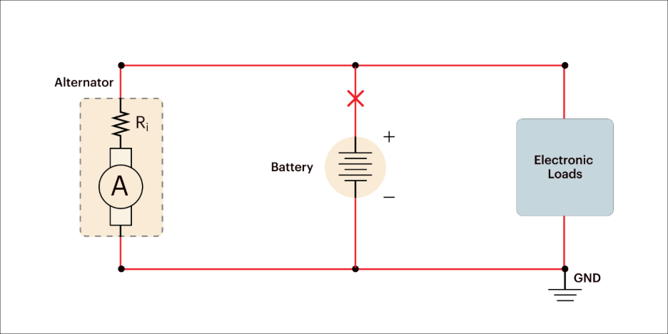
##### Figure 1 – Load Dump transient caused by battery disconnection
---
### 03
### ISO 16750-2 Test A and Test B Explained: Waveforms and Test Conditions
Automotive applications demand high reliability and safe operation. To address this, standards such as ISO 16750-2 define robust test conditions intended to simulate undesirable electrical transients that the circuit must be able to withstand through additional protection.
Compared with ISO 7637-2 which established lower voltage amplitudes and individual (non-repetitive) pulse test, ISO 16750-2 has more stringent conditions; emphasizing the need for careful and robust protection strategies to prevent damage and ensure long term system reliability.
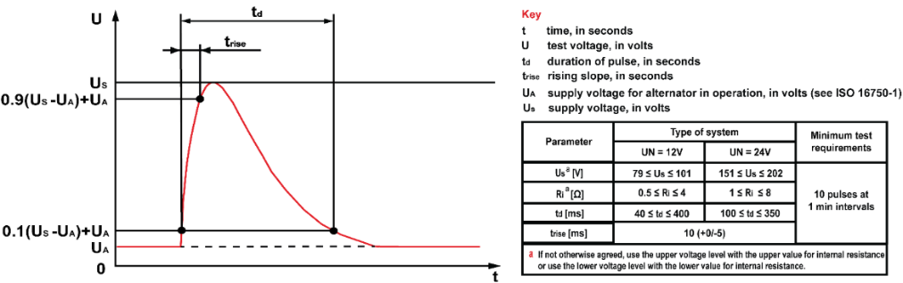
##### Figure 2 – Test conditions for Test A under ISO 16750-2
Test A in ISO 16750-2 specifies the parameters for the transient without centralized suppression with a minimum of 10 pulses at the specified interval. Amplitude can reach peak values of up to 101V for 12V systems and 202V for 24V systems.
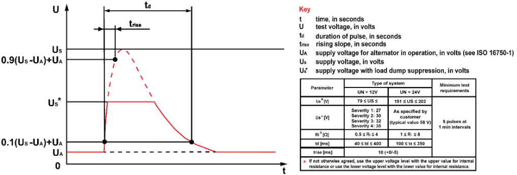
##### Figure 3 – Test conditions for Test B under ISO 16750-2
For Test B, the pulse shape and parameters are given according to an alternator with centralized load dump suppression, where for 12V systems the maximum surge voltage is described as Severity 4, (US = 35V), however, the exact value depends on the alternator technology, vehicle architecture, and any customer-specified severity levels. The minimum requirement for Test B is five pulses at a one-minute interval.
---
### 04
### Key TVS Selection Parameters for Automotive Load Dump Protection
The first step in selecting a suitable protection device is to define the minimum requirements the TVS diode must meet to withstand load dump transients. The following section summarizes the key TVS parameters.
- **Reverse Standoff Voltage or Reverse Working Maximum Voltage** (***V**RWM***)
The reverse working maximum voltage or reverse working maximum voltage is defined as the highest voltage the TVS diode can withstand in reverse bias without entering breakdown. This value must exceed the normal operating voltage of the system. According to ISO 16750-2, the maximum supply voltage (*USmax*) reaches 16 V for 12 V systems and 32V for 24V systems. These values must therefore be considered as the minimum required *VRWM* accounting for normal supply voltage variations.
- **Breakdown Voltage (*V**BR*)**
This is the voltage at which the TVS begins to conduct significantly, allowing it to clamp the surge and protect downstream circuitry. It lies between the *reverse working maximum voltage* (*VRWM*) and the *clamping voltage* (*VC*) and should be chosen above the maximum expected supply variations to avoid false triggering while ensuring fast response in this kind of transient.
- **Clamping Voltage (*V**C*)**
This parameter represents the voltage level seen by the protected circuit during a surge event; therefore, it must remain below the maximum allowable limit of the circuit to prevent system failure or the need for more robust and typically more costly components. Typical tolerance limits are approximately 37V–40V for linear regulators and 40V–60 V for DC-DC converters.
- **Peak Pulse Current (*I**PP*)**
The maximum current that the TVS diode can safely conduct for a specified surge waveform before thermal overload or failure occurs is called the *peak pulse current* (*IPP*). This is a critical selection parameter as TVS devices typically fail due to excessive current rather than excessive voltage.
- **Peak Pulse Power (*P**PP*)**
Finally, the surge absorbing capability of the selected device must be verified by ensuring that its rated power and pulse duration are matched to the surge conditions. This ensures the device can reliably withstand the event; where applicable, power derating should be applied.
- **AEC-Q101 Qualification**
AEC-Q101 is the automotive qualification standard for discrete semiconductors. TVS diodes qualified to AEC-Q101 have been validated for thermal, mechanical, and electrical reliability, making them suitable for automotive applications such as load dump protection, ECU protection, and power distribution systems.
These conditions allow for an initial screening of multiple part numbers and serve as guidance for the proper selection of the protection device. With these criteria established, the following TVS calculation can be performed, conducted to ensure compliance with ISO 16750-2, specifically for load dump pulses Test A and B.
Figure 4 illustrates the characteristic curve of a unidirectional TVS diode and shows the relationship between the key selection parameters discussed in this section, including *Reverse Working Maximum Voltage (VRWM), Breakdown Voltage (VBR)*, and *Clamping Voltage (VC)*.
Understanding how these parameters interact is essential when selecting a TVS diode for automotive load dump protection, as they directly influence the device's ability to remain inactive during normal operation while providing effective surge suppression during transient events.
The following overview is intended to support the load dump selection process presented in this application note. Readers seeking a more detailed explanation of TVS diode operation, characteristic curves, protection mechanisms, and parameter definitions are encouraged to refer to MCC's article, "[Understanding TVS Diodes: A Comprehensive Guide.](https://solutions.mccsemi.com/understanding-tvs-diodes-a-comprehensive-guide)"
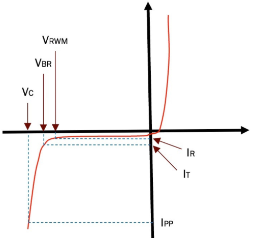
##### Figure 4 – Unidirectional TVS – Characteristic curve
---
### 05
### Step-by-Step TVS Selection Example for ISO 16750-2 Pulse 5A (12V System)
#### **Test conditions**
This calculation uses the upper voltage level and the maximum internal resistance as defined in ISO 16750‑2 for the Load Dump pulse. For a nominal 12 V system (*UN*), the parameters considered are a surge voltage of 101V (*VS*), pulse duration of 400ms (*td*), and the upper internal resistance value of 4Ω (*Ri*).

The maximum ambient temperature for this application is 105°C. For the maximum value of clamped voltage, we will consider 35V (*VC*), which is a typical high input voltage for voltage regulators and DC-DC converters in automotive design.
**1. Minimum *V**RWM***
The *reverse working maximum voltage* must account for battery voltage fluctuations. According to ISO 16750‑1, a 12V system can experience variations up to 16V; therefore, this value is used as the minimum required ***V**RWM.***
**2. Calculate** ***I**PP***
To calculate the *peak pulse current* due to the surge across the TVS we will use 𝐸𝑞. (1):
|  | (1) |
| --- | --- |
Where ***V**P*** is the *load dump surge voltage*, ***V**C*** is the *maximum clamping voltage* and ***R**i*** is the *internal resistance* from the alternator.
**3. Obtain** ***P**PP***
The *peak pulse power* across the protection device will be estimated considering the maximum ***V**C*** established and the calculated ***I**PP*** from the previous step:
|  | (2) |
| --- | --- |
**4. Calculate pulse duration (*tp*)**
Most protection-device datasheets define a pulse with (***t**d***), measured from 10% of the peak value and up to the point where decays to 50% of the *peak pulse current* (***I**PP***) as shown in Figure 5. This is the pulse shape used to measure peak-power pulse for all pulse widths shown in Figure 6.
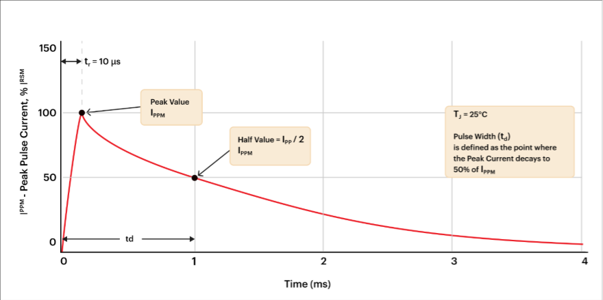
Figure 5 – Pulse Waveform – Peak Pulse Current
To align with the pulse-width definition shown in Figure 5, we need to find the load dump pulse duration at 50% of the *peak pulse current* (***I**PP***). This adjusted pulse duration is then used for power matching in the TVS selection process. For the calculation of this duration, we will use the equation of exponential decreasing voltage *Eq.* (3) similar to the discharge stage of a capacitor.
| 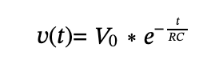 | (3) |
| --- | --- |
Where 𝒗(𝒕) is the *decreasing voltage across the TVS diode*, ***V**0*** represents the *surge voltage* and ***RC***the *constant of the equivalent circuit to discharge*. Fixing to fit the TVS parameters, we get:
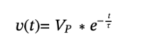(4)
By replacing ***t*** with the pulse duration***t**d***, the resulting equation becomes:
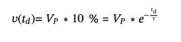
(5)
Where 10% is the voltage percentage from which we measure the transient duration.
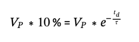
(6)
Dividing by ***V**P*** on both sides of the equation, we obtain:
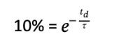
(7)
This expression is then solved to determine the time constant τ Here we use ***t**d*** = 390ms,
considering 10ms of rise time for the load dump pulse (as *Eq*. (3) only considers the decaying portion of the pulse)
.

(8)
Subsequently, to describe the decrease in current, we apply *Eq.(9)*.
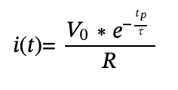
(9)
It is important to note that the protection device will start dissipating the excessive voltage once the surge exceeds the breakdown value of the TVS, therefore the subtraction of this value is added to the previous equation, with the corresponding adaptation of current parameters, as shown below:

(10)
From 𝐸𝑞.(10), the pulse duration ***t**p***is solved as below:

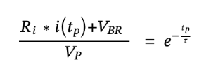
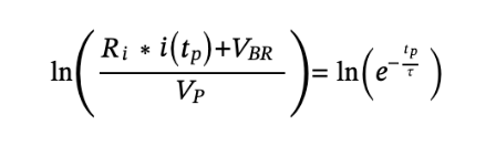
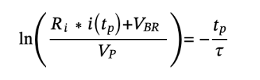
(11)
Lastly, in 𝐸𝑞.(11), ***i(t**p***) is set equal to corresponding to the 50% peak pulse current used in the pulse width definition, as previously shown in Figure 5. Using 𝐸𝑞.(11) with the known values of 𝜏=169ms, 𝑅𝑖=4𝛺, 𝐼𝑃𝑃=16.5𝐴, 𝑉𝑃=101𝑉, and using 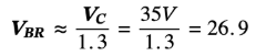to estimate the breakdown voltage, the following result is obtained:
 (12)
5. TVS power capability
At this stage, the Peak Pulse Power Rating Curve provided for each TVS family is used to select a device suitable for the calculated operating conditions. MCC offers the following Load-Dump-specific TVS series in the DO-218AB package:
1. SM8S series (6.6kW): [SM8S10(C)AHE3\_SM8S85(C)AHE3(DO-218AB).pdf](https://www.mccsemi.com/pdf/products/SM8S10(C)AHE3_SM8S85(C)AHE3(DO-218AB).pdf)
2. SM8Z series (8kW): [SM8Z10(C)AHE3\_SM8Z43(C)AHE3(DO-218AB).pdf](https://www.mccsemi.com/pdf/products/SM8Z10(C)AHE3_SM8Z43(C)AHE3(DO-218AB).pdf)
From the [MCC catalog](https://www.mccsemi.com/products/protection-devices/tvs), a TVS diode that is AEC‑Q101 compliant and qualified for load dump testing is selected. For this analysis, the [SM8SXX(C)AHE3](https://www.mccsemi.com/pdf/products/SM8S10(C)AHE3_SM8S85(C)AHE3(DO-218AB).pdf)family was chosen. From the corresponding Peak Pulse Power Rating Curve, the suitability of individual part numbers for the application can be evaluated. Then we determine the power capability of the device at the pulse width calculated through *Eq.*(12) obtaining a peak pulse power capability of 2000W at 88ms.
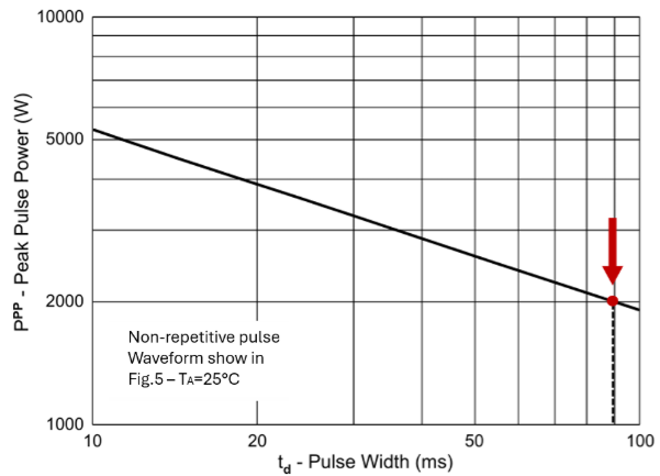
Figure 6 – Peak Pulse Power Rating Curve – SM8S10(C)AHE3 THRU SM8S85(C)AHE3
6\. Power derating
Increments in temperature impact the power capability of protection devices, thus a power derating must be applied to ensure a more reliable performance of the device. As previously noted, an ambient temperature of 105°C is used for this evaluation.
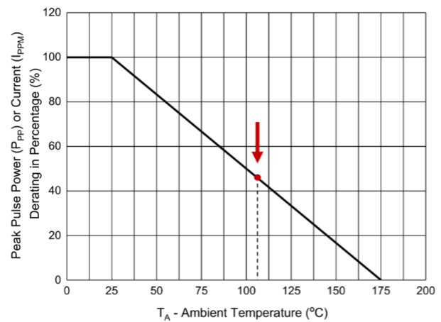
Figure 7 – Peak Pulse Derating Curve for Temperature – SM8S10(C)AHE3 THRU SM8S85(C)AHE3
The derating factor is approximately 45**%**; this value is applied to the previously determined peak pulse power to obtain the power capability at the application temperature:
 (12)
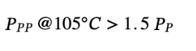
After applying power derating, the resulting ***P**PP*** @105°C remains higher than the peak pulse power calculated from Eq. (2) (577.5W) which represents the power dissipated across the TVS during the transient event. Based on this result, the calculation could be considered complete, as the protection device operates within a safe operating area even after temperature derating. Nevertheless, an additional step is included to further enhance robustness and provide an extra margin of protection.
**7. Component reliability on application**
As discussed in one of the application notes, [“Hot‑Swap Controller: Enhancing Data Center Reliability”](https://solutions.mccsemi.com/news/hot-swap-controller-application-note-enhancing-data-center-reliability) a successful protection strategy requires the TVS device to support a 50% safety margin over the peak pulse power (calculated in *Eq.* (2)) Accordingly,
|  | (14) |
| --- | --- |
Substituting values in *Eq.* (14) we get:
|  | (15) |
| --- | --- |
At this stage, it can be observed that the TVS family selected to protect against transient events in automotive applications, specifically the load dump, fulfills the power requirements to operate safely not only with the energy during the event but also with an additional margin as recommended for ensuring long-term reliability on our devices.
---
### 06
### Conclusions
Load dump is one of the most severe transient events encountered in automotive electrical systems, with surge amplitudes that can exceed 100V and durations lasting hundreds of milliseconds. As demonstrated throughout this application note, proper TVS diode selection requires more than simply choosing a device with a suitable voltage rating.
Parameters such as Reverse Working Maximum Voltage (VRWM), Breakdown Voltage (VBR), Clamping Voltage (VC), Peak Pulse Current (IPP), Peak Pulse Power (PPP), and AEC-Q101 qualification must all be considered to ensure reliable protection against ISO 16750-2 Test A and Test B load dump conditions.
Using the step-by-step calculation presented for a 12V automotive system, the selected [SM8S22CAHE3](https://www.mccsemi.com/products/protection-devices/tvs/sm8s22cahe3) TVS diode was shown to satisfy the voltage, current, power, temperature derating, and reliability margin requirements associated with the load dump transient.
This methodology provides a practical approach for engineers designing automotive ECUs, DC-DC converters, power distribution modules, and other electronic systems exposed to high-energy surge events.
However, analytical calculations alone do not fully describe the dynamic behavior of a TVS diode during a real load dump event. In Part 2 of this series, we will validate the calculation results using SPICE simulation and experimental test data.
The simulation will illustrate the transient voltage, clamping behavior, peak pulse current, and power dissipation of the selected TVS diode under ISO 16750-2 load dump conditions, allowing a direct comparison between theoretical calculations and real-world device performance.
---
### **07**
### **References**
- Micro Commercial Components (MCC). Understanding TVS Diodes: A Comprehensive guide. Retrieved from:
[https://solutions.mccsemi.com/understanding-tvs-diodes-a-comprehensive-guide](https://solutions.mccsemi.com/understanding-tvs-diodes-a-comprehensive-guide)
- Micro Commercial Components (MCC). (2025, May 13). Application Note: Enhancing Data Center Uptime with TVS Diodes in Hot-Swap Controllers. MCC - Application Notes. Retrieved from:
[https://solutions.mccsemi.com/news/hot-swap-controller-application-note-enhancing-data-center-reliability](https://solutions.mccsemi.com/news/hot-swap-controller-application-note-enhancing-data-center-reliability)
- Analog Devices. (2019, August 19). Load-Dump Protection for 24V Automotive Applications. Technical Articles. Retrieved from:
[https://www.analog.com/en/resources/technical-articles/loaddump-protection-for-24v-automotive-applications.html](https://www.analog.com/en/resources/technical-articles/loaddump-protection-for-24v-automotive-applications.html)
- Wang, Q. (2022). TVS Diode Selection and Theoretical Calculation in Automotive Electronics. Advances in Transdisciplinary Engineering, Volume 33: Mechatronics and Automation Technology, 10.3233/ATDE221218. Retrieved from: [https://doi.org/10.3233/atde221218](https://doi.org/10.3233/atde221218)
- International Organization for Standardization. (2011). ISO 7637-2:2011. ISO. Retrieved from:
[https://www.iso.org/standard/50925.html](https://www.iso.org/standard/50925.html)
- International Organization for Standardization. (2023). ISO 16750-2:2023. ISO. Retrieved from:
[https://www.iso.org/standard/77578.html](https://www.iso.org/standard/77578.html)
- International Organization for Standardization. (2023b). ISO 7637-1:2023. ISO. Retrieved from:
[https://www.iso.org/standard/83230.html](https://www.iso.org/standard/83230.html)
- Analog Devices. (2017, 5 April). LTspice: Models of ISO 7637-2 & ISO 16750-2 Transients (D. Eddleman, Ed.). Retrieved from:
[https://www.analog.com/en/resources/technical-articles/ltspice-models-of-iso-7637-2-iso-16750-2-transients.html](https://www.analog.com/en/resources/technical-articles/ltspice-models-of-iso-7637-2-iso-16750-2-transients.html)
- Bimbhra, P. S. (1999). Power Electronics (Third Edition). Khanna Publishers.
Micro Commercial Components, Corp., (MCC)
[Download the Application Note](https://solutions.mccsemi.com/hubfs/AN5001%20Load%20Dump%20Part%201%20PDF%20June%202026_v003.pdf)
###### Tags:
[Blog,](https://solutions.mccsemi.com/news/tag/blog) [Application Notes](https://solutions.mccsemi.com/news/tag/application-notes)
#### Related Content
[](https://solutions.mccsemi.com/news/application-note-quick-guide-on-automotive-load-dump-protection-iso-16750-2-part-2)
September 18, 2026
#### [Application Note: Quick Guide on Automotive Load Dump Protection (ISO 16750-2) - Part 2](https://solutions.mccsemi.com/news/application-note-quick-guide-on-automotive-load-dump-protection-iso-16750-2-part-2)
[](https://solutions.mccsemi.com/news/mcc-introduces-150w-aec-q101-tvs-diodes-for-automotive-protection)
February 23, 2026
#### [MCC Introduces 150W AEC‑Q101 TVS Diodes for Automotive Protection](https://solutions.mccsemi.com/news/mcc-introduces-150w-aec-q101-tvs-diodes-for-automotive-protection)
[](https://solutions.mccsemi.com/news/hot-swap-controller-application-note-enhancing-data-center-reliability)
May 9, 2025
#### [Application Note: Enhancing Data Center Uptime with TVS Diodes in Hot-Swap Controllers](https://solutions.mccsemi.com/news/hot-swap-controller-application-note-enhancing-data-center-reliability)
[](https://solutions.mccsemi.com/news/application-note-quick-guide-for-power-losses-calculation-in-mosfets-part-3)
May 27, 2026
#### [Application Note: Quick Guide for Power Losses Calculation in MOSFETs – Part 3](https://solutions.mccsemi.com/news/application-note-quick-guide-for-power-losses-calculation-in-mosfets-part-3)
.png?width=50&height=50&name=mcc%20150x150%20(1).png)
Post by [MCC](https://solutions.mccsemi.com/news/author/mcc)
July 8, 2026
MCC is a leading integrated device manufacturer (IDM) of discrete semiconductors worldwide. Headquartered in the US, we deliver supply chain assurance, best-in-class support, and a diverse portfolio of 10,000+ advanced components to help customers innovate in automotive, industrial, and beyond.
#### Global Headquarters
130 W Cochran St, Unit B
Simi Valley, CA. 93065
[818.701.4933](tel:%20818.701.4933)
---
#### Company
- [Company Profile](https://www.mccsemi.com/Home/CompanyProfile)
- [Products](https://www.mccsemi.com/ProductCategories)
- [Catalogs](https://www.mccsemi.com/Home/Catalogs)
- [Contact Us](https://www.mccsemi.com/Contact)
- [Careers](https://www.mccsemi.com/careers)
---
#### Explore
- [Events](https://www.mccsemi.com/events)
- [Quality](https://www.mccsemi.com/Quality/Index)
- [Blog](https://solutions.mccsemi.com/news/tag/blog)
- [News](https://solutions.mccsemi.com/news-events)
- [History](https://solutions.mccsemi.com/history)
- [Knowledge Center](https://solutions.mccsemi.com/knowledge-center)
---
#### Distributors & Customers
- [Log In](https://www.mccsemi.com/Account/Login)

[Complete Discrete Semiconductor Solutions  Powered by Service](https://solutions.mccsemi.com/)
[Terms of Sale and Export](https://www.mccsemi.com/Home/TermsAndConditions) [Privacy Policy](https://www.mccsemi.com/Home/PrivacyPolicy)
[Version : 1.0](https://www.mccsemi.com/Version)
MCC is a manufacturer of high-quality discrete semiconductors to the consumer markets © MCC. All Rights Reserved · 2026
```json
{
"@context": "http:\/\/schema.org\/",
"datePublished": "2026-07-08T3:40:45 PM",
"dateModified": "2026-09-21T9:26:47 PM",
"headline": "Application Note: Quick Guide on Automotive Load Dump Protection (ISO 16750-2)",
"description": "At Micro Commercial Components (MCC), we are committed to transparency, reliability, and continuous improvement for our global customers.",
"mainEntityOfPage": {
"@type": "WebPage",
"@id": "https://solutions.mccsemi.com/news/application-note-quick-guide-on-automotive-load-dump-protection-iso-16750-2"
},
"author": {
"@type": "Person",
"name": "MCC",
"url": "https://solutions.mccsemi.com/news/author/mcc"
},
"publisher": {
"@type": "Organization",
"name": "Micro Commercial Components",
},
"image": {
"@type": "ImageObject",
"url": "https://22710435.fs1.hubspotusercontent-na1.net/hubfs/22710435/brand-assets/Logo/MCC-favicon.gif"
},
"name": "Application Note: Quick Guide on Automotive Load Dump Protection (ISO 16750-2)"
}
```
```json
{
"@context" : "https://schema.org",
"@type" : "BlogPosting",
"author" : {
"@type" : "Person",
"name" : "MCC",
"url" : "https://solutions.mccsemi.com/news/author/mcc"
},
"dateModified" : "2026-09-21T21:26:47.362Z",
"datePublished" : "2026-07-08T15:40:45.000Z",
"headline" : "Application Note: Quick Guide on Automotive Load Dump Protection (ISO 16750-2)",
"image" : [ "https://solutions.mccsemi.com/hubfs/MCC_strenghten_its_future.png" ],
"mainEntityOfPage" : {
"@id" : "https://solutions.mccsemi.com/news/application-note-quick-guide-on-automotive-load-dump-protection-iso-16750-2",
"@type" : "WebPage"
},
"publisher" : {
"@type" : "Organization",
"logo" : {
"@type" : "ImageObject",
"url" : "https://solutions.mccsemi.com/hubfs/brand-assets/Logo/MCC%20Logo%201x.png"
},
"name" : "Micro Commercial Components"
}
}
```