.png?width=50&height=50&name=mcc%20150x150%20(1).png)
Approach to Estimate Total MOSFET Power Dissipation
In Part I of this application note series, equations were developed to estimate MOSFET turn-ON and turn-OFF switching intervals in hard-switching applications. These switching intervals form the basis for estimating switching power dissipation and comparing device performance under dynamic operating conditions.
In Part II, practical methods were introduced to extract key switching parameters from datasheet information, including plateau voltage approximation and equivalent capacitance estimation. These techniques help engineers apply switching loss calculations during early-stage device selection, even when detailed SPICE models are not available.
This third part of the series extends the previous analysis to a more complete MOSFET power loss evaluation. While switching losses are often one of the dominant contributors in high-frequency and high-power-density applications, they are not the only source of dissipation in a practical design. Conduction losses, output capacitance discharge losses, and gate driver losses must also be considered to obtain a realistic estimation of total device power dissipation.
This application note presents practical methods to estimate total MOSFET power losses in a low-side driver circuit with an inductive load. The analysis combines the switching interval calculations introduced in Part I with the datasheet-based parameter extraction methods developed in Part II. A complete calculation example using an MCC Power MOSFET is included and compared with simulation results to demonstrate the accuracy of the approach.
1. Introduction
As has been previously stated in past application notes of this series, power losses in MOSFET come from different sources, with switching time losses being one of the most important (see Figure 1a & 1b), especially in higher power density products.
Switching time losses are directly linked to the device’s dynamic parameters and hence, the importance of the right MOSFET.
However, a complete picture of Power Losses in a FET should include conduction, output capacitor discharge and gate-driver losses. These topics will be discussed here in detail and, at the end, a complete calculation example of complete Power Losses in a Low-Side Driver with Inductive Load will be presented.
%20ON%20state%20and%20a)%20OFF%20state..png?width=600&height=375&name=Figure%201.%20Switching%20Transition%20Waveforms%20for%20a)%20ON%20state%20and%20a)%20OFF%20state..png)
Figure 1 – Switching Transition Waveforms for a) ON state and b) OFF state
2. Types of Power Losses on MOSFETs
2.1 Switching time losses (ON and OFF)
This type of power loss occurs due to the MOSFET not being an ideal switch, but a practical one, meaning that it will not automatically go from vDS=VDD while in Off state and to vDS=I0rDS(on) while in ON state. Because of that, as shown in Figure 2 during ON/OFF transitions vDS≠0 and iDS≠0 occur simultaneously leading to power losses.
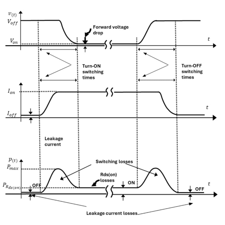 Figure 2 – Switching times and power losses
Using the results from previous Application Notes in this Series [1] the effective switching losses intervals are written as follows:

We can take Pon and Poff to be the peak power dissipated during ON and OFF transition respectively. Following a simplified and pessimistic triangular waveform shown in Figure 3 (instead of the actual waveform which has a smoother shape) will allow us to calculate the energy values using the area of the triangular waveform.

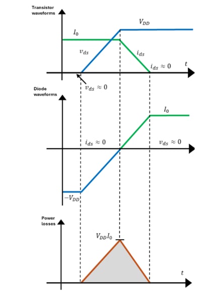
Figure 3 – Worst case for switching losses for MOSFET, where the gray area represents energy loss.
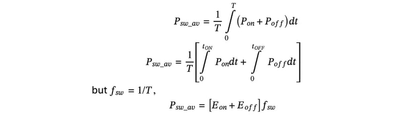
These switching losses are described in terms of energy, however, in several references in literature the switching losses are preferably described in terms of average power dissipation. Therefore, we can rewrite the following,
2.2 Conduction Losses
Figure 1 and Figure 2 show portions of time of the switching period where there are no switching power losses. These time intervals will involve other kinds of losses: conduction losses.
During the time interval before the MOSFET ON transition begins and the MOSFET is completely OFF, the device will draw a very small leakage current, given as Zero Gate Voltage Drain Current ( IDSS) in datasheets. In this document we will ignore these losses, nevertheless this small current exists.
In the other hand, when the MOSFET is completely ON (after turn-ON transition has completely passed and before turn-OFF transition begins; that is, after t3 in Figure 1a and before t1 in Figure 1b), vDS=I0rDS(on) and iDS=I0. This time interval is included in the complete Power Losses considering the time where the device remains at the ON-state, thus, the conduction power losses defined by energy are:
where D is the ON duty cycle (fraction of the switching period where the MOSFET is turned ON). This form of power conduction losses is included later in our calculation example. With the average conduction power losses given by:
2.3 Power losses due to 𝑪𝒐𝒔𝒔
The output capacitance Coss does not only affect the switching times or the plateau voltage but is also a source of power losses on its own. This is because the capacitor stores energy while the vDS is increasing, as seen in Figure 4. The discharge of Coss only happens while the device is turning ON, hence, the energy must be dissipated in form of power losses every time the MOSFET is activated .
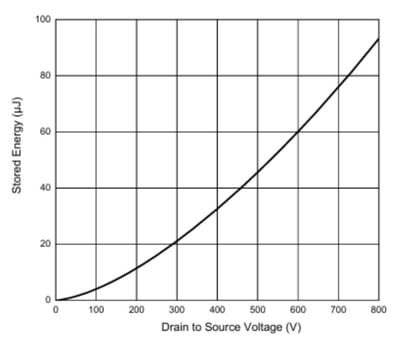 Figure 4.- Output capacitor stored charge.
The plot shown in Figure 4 is not always included in MOSFET datasheets, but there are ways to generate this plot from common datasheet information, this explored further in the document. But it is important to note that the energy losses due to Coss discharge are found with the analysis below, which consist in basic analysis of power in a circuit in energy equations, given by:

where P is the power being integrated for a given time t. But we can define: 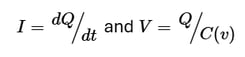 for a capacitor (in this case a non-linear capacitor C(v). Therefore, energy expression is also:

To avoid complex solutions to this equation, the non-linear capacitor can be replaced with an equivalent linear capacitor. Section 3.2 will show how to obtain this equivalent linear capacitor, named here Coss. Thus, solving the integral above we have:

Then, the average power dissipated due to discharging the MOSFET’s Output Capacitor is:
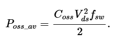
2.4. Gate driver power losses
For this application note, the typical threshold voltage defined in the datasheet is used. No detailed calculation method was found in the literature.
In addition, manufacturers typically use the same measurement conditions, namely VDS=VGS, ID=250µA, which makes comparison between devices more straightforward (Figure 8).
For the transistor to turn on and off, it is necessary to have a circuit driver at its gate terminal. Up to this point, we have only analysis transition losses, but the energy to charge and discharge the gate capacitor should come from somewhere. There are plenty of gate driver circuits in several shapes and forms, here it is represented as a Thevenin equivalent in the example circuit used, see Figure 5.
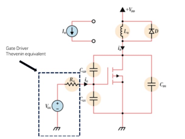
Figure 5 - Low side driver circuit with inductive load and Thevenin equivalent at gate terminal.
Following the same analysis done in the previous section with Coss, we can obtain the energy needed to charge MOSFET input capacitance Ciss as (these losses happen during both transitions and the divided by 2 factor disappears):


Finally, the total average power losses can be written as:

3. Energy Related equivalent output capacitance 𝑪𝒐𝒔𝒔_𝒆
As mentioned before in this series, Ciss and Coss are non-linear capacitances which values strongly depends on VGG and VDD. These non-linearities complicate the calculations since vGD swings from VDD(off) to −VGG(on) and vDS swings from VDD(off) to vDS(on) ≈ I0rDS(on).
For the estimation of the energy related equivalent output capacitance Coss_er, the extraction method detailed in Part 2 of this series [2] can be used. The objective is to find an equivalent linear capacitor value with the same energy related to the non-linear capacitor energy at the desired VDS. To do this, data points in the Coss capacitance small signal characteristics need to be extracted from the datasheet plot and used to simulate the non-linear charge curve with respect to its terminal voltages using the method in [3] and explained in [4]. This simulation can be used to obtain the plot of the Non-Linear Coss storage energy with respect to VDS as shown in Figure 4, and using the following equation, which is derived by the principles stated in [5], and what is seen in Figure 6, where the lined area corresponds to the stored energy:

Given that, using the following capacitor definition, we can obtain an equivalent linear capacitor with the same energy as the non-linear capacitor Coss at a specific VDS voltage:

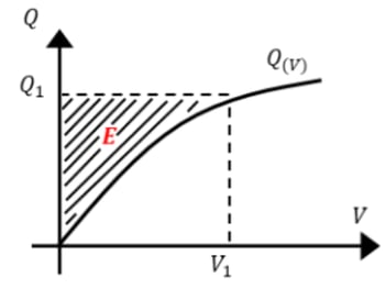
Figure 6. Energy stored in Non-linear capacitor can be found as the shaded area in this plot.
4. Power Losses Calculation
As an example, following the procedure previously described above, a calculation for power losses will be done under the analysis of an LSD with an inductive load.
Taking the following values for surrounding conditions on Figure 5 Low-Side driver circuit: VGG=10V, VDD=75V, Io=15A, Rgext=10Ω an example calculation will be presented here.
For this MCC’s Power MOSFET MCAC15N15Y will be used.
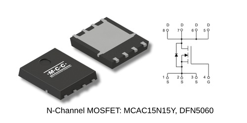
Table 1 shows these component parameters that are relevant for this analysis.
|
Parameter |
Symbol |
Conditions |
|
|
Drain-Source Maximum Voltage |
VDS |
150V |
VGS=0V, ID=250μA |
|
Gate-Threshold Voltage |
VGS(th) |
2V to 4V |
VDS=VGS, ID=250µA |
|
Drain-Source On-Resistance |
rDS(on) |
52mΩ (typ) 70mΩ (max) |
VGS=10V, ID=15A |
|
Internal Gate Resistance |
Rgint |
1Ω |
f=1MHz, Open drain |
|
Gate-Drain Charge |
QGD |
4nC |
VDS=75V, VGS=10V, ID=15A |
|
gm |
14.86643 |
125°C |
|
|
gm |
23.70255 |
25°C |
Table 1. Electrical parameters for MCAC15N15Y relevant for calculations.
The parameters referent to device driving are switching frequency  and the duty cycle D=80%.
Firstly, it is necessary to calculate equivalent capacitance with
 The Coss is obtained simply using the parameter Eoss=388.11037nJ extracted from simulation like

The Ciss is taken directly from the datasheet as it’s the only capacitance that remains with nearly linear behavior despite the voltage applied. For this example,Ciss=740pF.
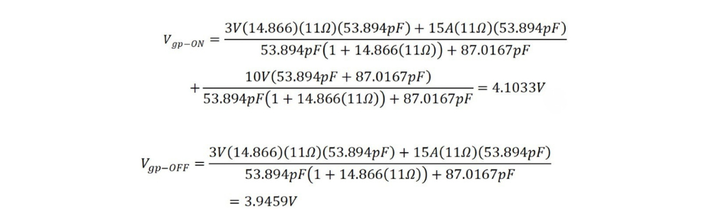
After that, it is now possible to calculate Vpon and Vpoff with equation below. The result is


Now, the calculation for the times intervals tON and tOFF is written as
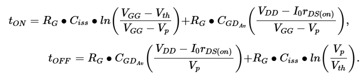

 13.3817ns
Following with the process described in the document, now it is possible to calculate the energy dissipated due to switching of the transistor:
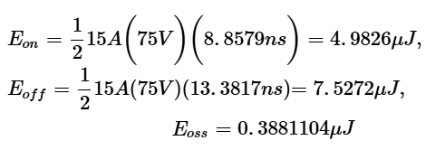
and then get the average power dissipation by multiplying by the switching frequency like

Conduction and driver power losses are also included in the average power losses of the device. Using the values from the datasheet and application circuit we have


Thus, the total average power losses due to MOSFET are

5. Simulation
|
|
𝒕𝑶𝑵=𝒕𝟐𝟏𝑶𝑵+𝒕𝟑𝟐𝑶𝑵
|
𝒕𝑶𝑭𝑭=𝒕𝟐𝟏𝑶𝑭𝑭+𝒕𝟑𝟐𝑶𝑭𝑭
|
Power Losses |
|
Simulation |
9.86ns |
8.17ns |
9.4324W |
|
Calculation |
8.8579ns |
13.3817ns |
9.448W |
Table 2. Comparison between simulation and calculation results of switching times and power losses for MCAC15N15Y.
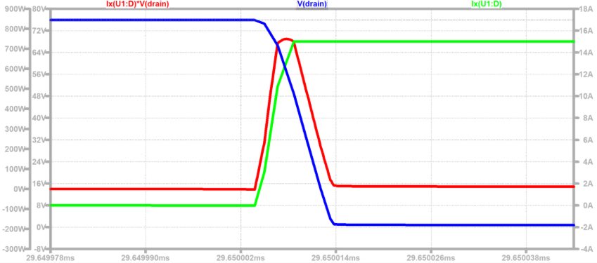 |
| Figure 7. Turn-ON waveform for MCAC15N15Y in ltspice. The red waveform corresponds to the power losses due to the switching between ON and OFF. |
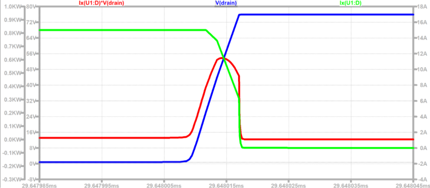 |
| Figure 8. Turn-OFF waveform for MCAC15N15Y in ltspice. The red waveform corresponds to the power losses due to the switching between OFF and ON. |
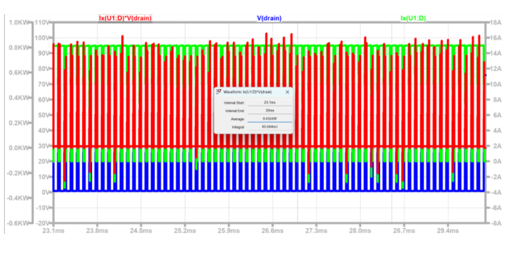 |
| Figure 9. Average power losses for the MCAC15N15Y. |
6. Conclusions
In this application note, a calculation approach for estimating total losses in power MOSFET switching applications was presented. With this approach, conduction and switching losses can be evaluated and compared during component selection. Achieving low RDS(on) while maintaining strong dynamic characteristics is often a design trade-off, and this analysis helps determine the optimal balance.
Additionally, the procedure presented here allows designers to identify the main contributors to switching losses, including transition times where drain-to-source voltage and current overlap, output capacitance discharge, and gate driving losses. This becomes increasingly important as switching frequencies continue to rise due to the industry trend toward higher power density.
Finally, a simulation example was presented to demonstrate how closely this simplified analysis matches full electrical model simulations, allowing the approach to be used for worst-case analysis and component comparisons without significantly compromising accuracy.
References:
- [1] Erickson, R. W., & Maksimović, D. (2020, p. 123). Fundamentals of Power Electronics (3.a ed.). Springer.
- [2] MCC. (2026). Application Note: Quick guide for power losses calculation in MOSFETS – Part 2. Micro Commercial Components Corp.. Section 2.2
- [3] I. Zeltser and S. Ben-Yaakov, "On SPICE Simulation of Voltage-Dependent Capacitors," in IEEE Transactions on Power Electronics, vol. 33, no. 5, pp. 3703-3710, May 2018, doi: 10.1109/TPEL.2017.2766025.
- [4] Sam Ben-Yaakov. (2018, 24 enero). Deciphering Coss of power MOSFETs .
- [5] U. Jadli, F. Mohd-Yasin, H. A. Moghadam, J. R. Nicholls, P. Pande and S. Dimitrijev, "A Simple Equation for the Energy Stored by Voltage-Dependent Capacitances," in IEEE Transactions on Power Electronics, vol. 35, no. 12, pp. 12629-12632, Dec. 2020, doi: 10.1109/TPEL.2020.2993639.