.png?width=50&height=50&name=mcc%20150x150%20(1).png)
Approach to Estimate Switching Time Intervals Using Datasheet Parameters
In Part I of this application note series, a practical framework was introduced to estimate switching power losses in Power MOSFETs by calculating turn-ON and turn-OFF time intervals. These equations provide a useful first-order method for evaluating switching behavior in hard-switching applications using a simplified driver model.
However, applying these equations in real design scenarios quickly reveals a common challenge: several key parameters required for the calculations are strongly dependent on operating conditions and are not always directly available from datasheets in a form suitable for comparison.
This second part of the series addresses that gap.
1. Introduction
In Part I of this series, equations were developed to calculate MOSFET turn ON and turn OFF switching time intervals. These time intervals form the basis for switching power loss calculations in hard switching applications.
When applying these equations, it becomes evident that additional guidance is required. Several parameters used in the calculations, particularly gate plateau voltage and parasitic capacitances, depend strongly on operating voltage and current conditions. These parameters are not always directly available for the intended use case.
This application note provides practical methods to estimate these parameters using commonly available datasheet information. Approaches for plateau voltage approximation, reverse transfer capacitance extraction, and output capacitance modeling are presented. These methods enable consistent comparison of MOSFET switching behavior across suppliers when detailed SPICE models are not available.
The techniques described in this Part II are intended for component level comparison and early-stage device selection. When the objective is application-level loss modeling or worst-case analysis, time domain simulation using validated SPICE models remains the preferred approach.
1.1 ON and OFF time intervals
From Part I of this series, time intervals for the turn-ON transition are given as follows:
 |
| Formula 1 |
 |
| Formula 2 |
 |
| Formula 3 |
In addition, the turn-OFF transition time intervals were found to be:
 |
| Formula 4 |
 |
| Formula 5 |
 |
| Formula 6 |
Where τ=RG(CGS+CGD), the time intervals are defined as in Figure 1, and the following parameter definition apply:
|
RG: Gate resistance (internal and external). CGS: Parasitic Gate-to-Source Capacitance. CGD: Parasitic Gate-to-Drain Capacitance. RDS(on): Drain-to-Source resistance when MOSFET is fully-ON. Vth: Threshold Voltage. |
Vgp−ON: Plateau Voltage during ON transition. Vgp−OFF: Plateau Voltage during OFF transition. VGG: Gate external voltage supply DC value. VDD: Drain external voltage supply DC value. Io: Drain load DC current. |
Formulas 1-6 were derived from a Low-Side Driver sample circuit with inductive load and ideal recirculating diode as the one shown in Figure 2.
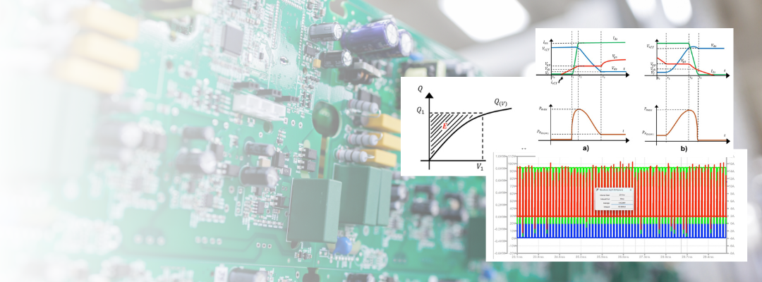
| Figure 1a: Turn-On MOSFET Waveforms | Figure 1b: Turn-Off MOSFET Waveforms |
 |
 |
Figure 1 – Switching Transition Waveforms

Figure 2 – Low-Side Driver Sample Circuit
2. Parameter approximations
2.1 Plateau Voltage for ON and OFF stages
It is clear from equations 2-4 and 6 that Gate Plateau Voltage is a parameter of high importance. However, deciding what voltage to use is often difficult.
Datasheet will show a Plateau Voltage under a determined set of conditions of Drain Voltage and Current. This value can be extracted from the datasheet Gate Charge plot to be used for calculations (Figure 3).

Figure 3 – Typical Gate Charge plot from Power MOSFET datasheet
Nevertheless, conditions for measuring Plateau Voltage are not standard and therefore looking for an approximation that considers surrounding conditions makes sense.
According to [1] Plateau Voltage might even be different depending if the device is turning OFF or turning ON, and it will be defined by the following equations:
 |
| Formula 7 |
 |
| Formula 8 |
Where gm is the transconductance obtained from the slope of the linear portion of the Transfer Characteristics (Figure 4).
Equations 7 and 8 are an option to derive Plateau Voltages for ON and OFF stages that bring datasheet Plateau to closer reference conditions for parameter comparison of two or more Power MOSFET Part-Numbers.

Figure 4 – Typical Transfer Characteristics Plot from Power MOSFET datasheet
2.2 Reverse Transfer Capacitance (𝑪𝒓𝒔𝒔)
From Part I of this series, we know that Reverse Transfer Capacitance Crss is equal to CGD which is a major parameter for equations 3 and 5. CGD can be obtained by using Gate-Drain charge, QGD, from datasheet dynamic characteristic tables, which lets the following formula to be applied:
 |
| Formula 9 |
When using this method, it needs to be considered that QGD is obtained with a determined VGS value different from zero and that CGD non-linear capacitor is both dependent on VGS and VDS bias values (Figure 5)
 .
.
Figure 5. Example of Gate-Drain Charge from Power MOSFET Datasheet
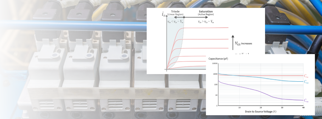
Another way of approaching this capacitance will let us have values obtained from a standard method [3] that uses same measurement conditions making component comparison more trustable. Crss characteristics plot, Figure 6, is obtained with a sweep of bias voltages for VDS with added small signal vds high frequency disturbances (i.e. capacitances in Figure 6 are small signal capacitances). It is worth noting that is an industry standard to have VGS = 0V during this characterization.

Figure 6 – Example MOSFET Small-Signal Capacitance plots from Datasheet
From this plot, we can read the Crss=CGD value to desired VDS voltage and use it for time interval calculations. That is one valid way of doing it, sufficiently good for comparison purposes. Alternative way is to find an equivalent linear capacitor value related to the charge on the non-linear capacitor at the desired VDS. To do this, all points in the Crss capacitance characteristics need to be extracted and used to simulate the non-linear charge curve with respect to its terminal voltages using the method in [2]. CGD is then obtained applying formula (9). These last two methods allow us to have CGD values for all MOSFETs in comparison that use the same VDS and VGS bias conditions.
This last simulation step can be regarded as an unnecessary extra step if the analysis goal is just to compare component performance. However, having this simulation allows detailing the non-linear capacitors more completely as is shown in Figure 7.
 |
| Figure 7 – Non-linear capacitor charge curve (Cd – small signal capacitance at Vx, Ct – equivalent linear capacitor at Vx) |
2.3 Output Capacitance (𝑪𝒐𝒔𝒔)
Once CGD is defined, the same approach can be taken for CDS. In similarity with Crss, Output Capacitance Coss is defined in Figure 6 plot. Same benefit of having measurements with a well stablished method is accomplished, this makes conditions between suppliers similar and comparable.
The value of CDS is obtained after applying the following subtraction:
 |
| Formula 10 |
Where, as was detailed above, Coss can be read directly from the small signal non-linear capacitance plot (Figure 5) or the points from this characteristic can be extracted to simulate the non-linear charge curve with respect to Drain-to-Source voltage [2] and use:
 |
| Formula 11 |
2.4 Gate-Threshold Voltage (Vth)
For this application note, the typical threshold voltage defined in the datasheet is used. No detailed calculation method was found in the literature.
In addition, manufacturers typically use the same measurement conditions, namely VDS=VGS, ID=250µA, which makes comparison between devices more straightforward (Figure 8).

Figure 8 - Typical Gate-Threshold Datasheet table
3. Calculation example
3.1 Sample circuit
Taking the following values for surrounding conditions on Figure 1 Low-Side driver circuit:
VGG =1 0V, VDD = 75V, Io =1 5A, Rgext = 10Ω
an example calculation will be presented here.
For this MCC’s Power MOSFET MCAC15N15Y will be used along with two competitor MOSFETs that are close in electrical characteristics. Table 1 and Table 2 show these component parameters that are relevant for this analysis.
|
Parameter |
Symbol |
Conditions |
|
|
Drain-Source Maximum Voltage |
VDS |
150V |
VGS=0V, ID=250μA |
|
Gate-Threshold Voltage |
VGS(th) |
2V to 4V |
VDS=VGS, ID=250µA |
|
Drain-Source On-Resistance |
rDS(on) |
52mΩ (typ) 70mΩ (max) |
VGS=10V, ID=15A |
|
Internal Gate Resistance |
Rgint |
1Ω |
f=1MHz, Open drain |
|
Gate-Drain Charge |
QGD |
4nC |
VDS=75V, VGS=10V, ID=15A |
|
Plateau-Voltage |
Vp |
4.9V |
VDS=75V, ID=15A |
|
Input Capacitance |
Ciss=CGS+CGD |
749.9pF |
VDS=30V, VGS=0V, f=1MHz |
|
Output Capacitance |
Coss=CDS+CGD |
301.1pF |
VDS=30V, VGS=0V, f=1MHz |
|
Reverse Transfer Capacitance |
Crss=CGD |
27.3pF |
VDS=30V, VGS=0V, f=1MHz |
Table 1. Electrical parameters for MCAC15N15Y relevant for calculations.
|
Symbol |
Competitor A |
Conditions |
Competitor B |
Conditions |
|
VDS |
200V |
VGS=0V, ID=250μA |
150V |
VGS=0V, ID=250μA |
|
VGS(th) |
2V to 4V |
VDS= VGS, ID=1mA |
2V to 4V |
VDS= VGS, ID=35µA |
|
rDS(on) |
86mΩ (typ) 102mΩ (max) |
VGS=10V, ID=12A |
42mΩ (typ) 52mΩ (max) |
VGS=10V, ID=18A |
|
Rgint |
1.1Ω |
f=1MHz |
2.1Ω |
f=1MHz |
|
QGD |
10.1nC |
VDS=100V, VGS=10V, ID=12A |
1.5nC |
VDS=75V, VGS=10V, ID=9A |
|
Vp |
4.5V |
VDS=100V, ID=12A |
5.2V |
VDS=75V, ID=9A |
|
Ciss=CGS+CGD |
1568pF |
VDS=30V, VGS=0V, f=1MHz |
670pF |
VDS=75V, VGS=0V, f=1MHz |
|
Coss=CDS+CGD |
170pF |
VDS=30V, VGS=0V, f=1MHz |
80pF |
VDS=75V, VGS=0V, f=1MHz |
|
Crss=CGD |
55pF |
VDS=30V, VGS=0V, f=1MHz |
3.4pF |
VDS=75V, VGS=0V, f=1MHz |
Table 2. Electrical parameters for competition that are relevant for calculations.
3.2 LTspice Simulation of Sample Circuit
Simulations using SPICE models from MCAC15N15Y and Competition were performed. From simulation results measured time intervals tON = t21ON + t32ON and tOFF = t21OFF + t32OFF are going to be used in this analysis as a reference. Results are shown in Table 3. Figure 9 shows tON measurement from simulations taken from the point where the 5% of maximum Drain current is reached (0.05∗Io=0.75A) to the point where 5% of the maximum Drain voltage is reached (0.05∗VDD=3.75V). Same points, but with voltage appearing first than current were taken to measure tOFF (Figure 10).
|
MCAC15N15Y |
Competitor A |
Competitor B |
Δ (MCC – Competition) |
||
|
A |
B |
||||
|
tON=t21ON+t32ON |
8.68ns |
18.40ns |
5.46ns |
-9.72ns |
3.22ns |
|
tOFF=t21OFF+t32OFF |
12.43ns |
23.00ns |
5.91ns |
-10.57ns |
6.52ns |
Table 3. Turn-on and turn-off times obtained from simulation measurements
 |
| Figure 9. MCAC15N15Y Turn-on time from Simulation (Io in green, VDS in dark blue & VGG in light blue) |
 |
| Figure 10. MCAC15N15Y Turn-off time from Simulation (Io in green, VDS in dark blue & VGG in light blue) |
3.3 Calculation Using Datasheet Values
Calculations using datasheets values shown in Table 1 and Table 2 were used to calculate results in Table 4.
|
|
MCAC15N15Y |
Competitor A |
Competitor B |
Δ (MCC – Competition) |
|
|
A |
B |
||||
|
t10ON |
2.94ns |
6.26ns |
2.91ns |
- - |
- - |
|
t21ON |
2.61ns |
4.24ns |
3.08ns |
- - |
- - |
|
t32ON |
4.37ns |
8.26ns |
2.02ns |
- - |
- - |
|
tON = t21ON+t32ON |
6.98ns |
12.49ns |
5.1ns |
-5.51ns |
1.88ns |
|
t10OFF |
5.89ns |
14.02ns |
5.33ns |
- - |
- - |
|
t21OFF |
4.55ns |
10.09ns |
1.87ns |
- - |
- - |
|
t32OFF |
4.05ns |
7.12ns |
4.48ns |
- - |
- - |
|
tOFF = t21OFF+t32OFF |
8.60ns |
17.21ns |
6.35ns |
-8.61ns |
2.25ns |
Table 4. Calculation results using datasheet values.
3.4 Calculation Using Plateau Voltage
Modeling approach of Plateau Voltage described in Section 2.1 was used to obtain results shown in Table 5.
|
|
MCAC15N15Y |
Competitor A |
Competitor B |
Δ (MCC – Competition) |
|
|
t10ON |
2.94ns |
6.33ns |
2.91ns |
- - |
- - |
|
t21ON |
1.22ns |
1.35ns |
1.80ns |
- - |
- - |
|
t32ON |
3.69ns |
7.00ns |
1.73ns |
- - |
- - |
|
tON = t21ON+t32ON |
4.91ns |
8.35ns |
3.52ns |
-3.44ns |
1.39ns |
|
t10OFF |
8.60ns |
18.78ns |
8.99ns |
- - |
- - |
|
t21OFF |
6.32ns |
13.23ns |
2.92ns |
- - |
- - |
|
t32OFF |
1.33ns |
2.36ns |
0.82ns |
- - |
- - |
|
tOFF = t21OFF+t32OFF |
7.65ns |
15.59ns |
3.75ns |
-7.94ns |
3.90ns |
Table 5. Calculation results using Plateau Voltage model (Section 2.1)
4. Conclusions
Comparing the switching performance of Power MOSFETs across different manufacturers, or between part numbers from the same manufacturer, remains inherently challenging. Variations in measurement conditions directly influence reported device parameters and, as a result, affect any switching performance prediction.
As introduced in Part 1 of this series, accurate switching loss estimation begins with understanding the turn-ON and turn-OFF transitions in low-side driver configurations with inductive loads. Building on that foundation, this application note demonstrated that both direct use of datasheet values and the plateau voltage modeling approach provide reliable results for comparative analysis. Each method offers a practical approximation of relative switching speed, enabling meaningful comparison of how quickly one device transitions relative to another.
Comparisons derived from either approach give a clear indication of relative switching performance when devices are evaluated under equivalent operating conditions. The plateau voltage modeling approach presented in this work further improves consistency by normalizing comparisons to a common reference point, which is particularly valuable when published plateau voltage specifications are measured under differing test conditions.
Part 3 of this series applies these calculated parameters to estimate total MOSFET power dissipation by combining switching and conduction losses in a practical high-side driver application example.
References:
-
[1] Liu, S., Song, S., Xie, N., Chen, H., Wu, X., & Zhao, M. (2021). Miller Plateau Corrected with Displacement Currents and Its Use in Analyzing the Switching Process and Switching Loss. Electronics 2021, 10
-
[2] Ben-Yaakov, S. & Zeltser, I. (2017). On SPICE simulation of voltage dependent capacitors. IEEE Transactions in Power Electronics
-
[3]JEDEC SOLID STATE TECHNOLOGY ASSOCIATION (1985). JESD24 JEDEC Standard for Power MOSFETs