.png?width=50&height=50&name=mcc%20150x150%20(1).png)
Best Practices for Integrating TVS Diodes in Hot-Swap Systems
Data centers are facing a critical challenge due to the rapid expansion of cloud computing services and the proliferation of artificial intelligence (AI). This unprecedented growth has resulted in an increased demand for data processing, which, in turn, heightens the need for robust power management systems. A significant concern is the risk of power supply failures, which can lead to widespread system outages, resulting in data loss and substantial downtime.
To address this issue, data centers have implemented hot-swap devices that allow specific server application boards to be added or replaced without shutting down the system. However, these solutions are not enough on their own. To fully ensure reliability and protect against transient current and voltage surges, it is indispensable to incorporate transient voltage suppressors (TVS diodes) into hot-swap controllers.
In this application note, we will outline a procedure for selecting an appropriate TVS device for hot-swap applications, aiming to mitigate the risks associated with power supply failures and enhance overall system reliability.
Data Center Specifications and Requirements
Data center circuits are highly complex. However, when analyzing the power supply architecture, the block diagram can be simplified for clarity, as shown in Figure 1.

Fig. 1. Block diagram 54V DC-based power supply architecture.
Traditionally, power supply systems in data centers and servers have relied on a 12V DC-based architecture. However, with the rapid increase in data management requirements and power density, the demand for higher efficiency in power delivery has become crucial. This complexity is compounded as data centers transition to a 48V to 54V DC architecture, which is now becoming standard in telecommunications and IT systems.
This shift to a higher voltage output from AC/DC converters is not merely a change in numbers — it significantly affects current flow and loss minimization, thereby improving overall efficiency. The transition reflects the multifaceted challenges data centers face in optimizing their power management systems while accommodating growing demands.
Hot-Swap Systems and the Challenges of Transient Voltage Surges
The primary goal of data center operations is to maintain continuous activity without interruptions. To achieve this, uninterruptible power supply (UPS) systems are put in place to ensure that the underlying power system remains operational under any circumstances, effectively preventing failures.
However, the DC block can experience issues such as server disconnections that are unrelated to power supply failures, leading to problems from transient parasitic inductance and capacitance effects, which create a precarious situation for data center reliability.
To manage capacitive in-rush currents, hot-swap circuits control current peaks that could damage connected servers during board swapping. These circuits, as seen in Figure 1, safely disconnect a failed server by turning off MOSFET Q1 to avoid overcurrent damage in case of a failed load.
Still, having a proper hot-swap design will not prevent parasitic inductances from the backplane to the swap card connection to cause an inductive kickback when a faulty load is disconnected. This phenomenon occurs because the overcurrent detected by the hot-swap controller will still try to flow during load disconnection, leading to arcing risk.
To prevent damage, this overvoltage must be diverted from the circuit and discharged safely. This is why TVS diodes are indispensable. The TVS diodes must be connected in parallel with the power supply to provide adequate protection during inductive overvoltage transients. These clamping diodes will protect the system by limiting the voltage using the avalanche effect.
Choosing an Appropriate TVS: 9-Step Approach
Step 1:
Select a minimum standoff voltage VR. This will be equal to or greater than the DC or continuous peak operating bus voltage level plus a selected tolerance. In this case, a 5% tolerance was considered:

Step 2:
Obtain maximum expected pulse current IP. For this step, the designer must do an analysis of the whole circuit and a worst-case analysis for the application.
The analysis would include parasitic inductance effect, threshold current point for the specific hot-swap controller, tolerance of the shunt resistor or current mirror used for overcurrent detection, and the worst-case time is expected to take the controller to shut off the application.
In this example, a peak current of 480A is used.
Step 3:
At this point, the designer should preselect some TVS with the stablished working voltage in Step 1. MCC’s SMC 5kW series offers robust TVS options and the following set of part numbers meet the standoff voltage requirement. We will evaluate them for this application:
Step 4:
Next step is finding the clamping voltage 𝑉𝐶 for the transient. The following equation is used:

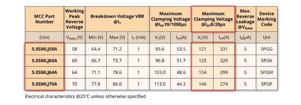
Here, 𝐼𝑃 is the estimated level from Step 2. 𝐼𝑃𝑃, 8/20𝜇𝑠, and 𝑉𝐶(𝑀𝑎𝑥),8/20𝜇𝑠 are the values in the datasheet for the 8/20 µs pulse standard test in accordance with IEC 61000-4-5. This is the shorter pulse included in the datasheet, and it is selected because this will be closer to the expected transient time for a hot-swap IC protection situation. 𝑉𝐵𝑅 is given in the datasheet. Below is an example calculation for 5.0SMLJ60A:

Fig. 2. Table with the important parameters from the datasheet for the 5.0SMLJxxxx TVS series.
Step 5:
After that, the calculated 𝑉𝐶 from previous step and the estimated 𝐼𝑃 are used to find power across the TVS during the transient pulse:

The actual voltage and current values must be measured directly on the circuit to confirm they align with the maximum peak power level found here.
Step 6:
The pulse duration ∆𝑡𝑑 will be estimated using the input parasitic inductance in the equation below. This parasitic inductance is related to the PCB traces and cabling connection from backplane to the hot-swap board:

Here, ∆𝑖𝐿 is the current across the inductor during the pulse, ∆𝑖𝐿= 𝐼𝑃−0𝐴 is considered because 𝐼𝑃 is the initial current condition and the pulse time will be calculated for the complete discharge. Solving for∆𝑡𝑑:

And using the values obtained in previous steps, the following time is obtained for this example:

Step 7:
In this and the next step, the power capabilities of a single TVS will be found. The allowable peak pulse power 𝑃𝑃𝑃 for the pulse duration ∆𝑡𝑑 of Step 6 is shown in Figure 3. The power that the component can dissipate is slightly greater than 80 kW.
Fig 3. Peak pulse power rating curve for the 5.0SMLJxxxx TVS.
Step 8:
Up to this point, the next step is to derate the allowable 𝑃𝑃𝑃 to account for the maximum ambient temperature expected in the application. It is suggested to include heating effects caused by nearby components. In Figure 4, a maximum temperature of 125°C is shown.
Fig 4. Peak pulse derating curve for temperature for the 5.0SMLJ60A TVS.
In this example, the final maximum allowable power for the component after derating is:
.png?width=1000&height=80&name=Step%208%20final%20maximum%20allowable%20power%20for%20the%20component%20after%20derating%20is%20-%20mcc%20semi%20-%20micro%20commercial%20components%201000x80%20(1).png)
Step 9:
For a TVS to be successful, the total derated power of Step 8 must be above the calculated TVS peak power from Step 5 with a margin of at least 50% to ensure the reliability of the component and the application:

In this example the result is the following:

The power condition is not met, and a new iteration of this 9-step process for TVS selection should follow. However, there are two solutions:
a. Another device with greater power capabilities is analyzed.b. Use a few of the same TVS components in parallel to divide power.
In a following application note, a simulation approach will be presented where option (b) is explored.
Table 1 summarizes the calculation for three different 𝐼𝑃 values, 120A, 160A, and 480A. Cases in green are successful in meeting the power condition given in Step 9 with a single device.
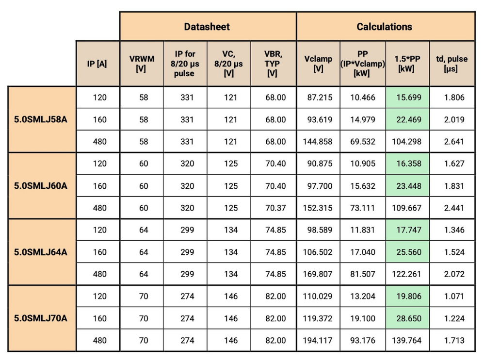
Table 1. Datasheet parameters and calculated 𝑃𝑃 and td values for TVS devices from the 5.0SMLJxxxx MCC‘s series showing the parameters found in the datasheet and from calculations shown in this work.
Sources:
- Flex Power Modules. (n.d.). Optimizing power electronics for AI. Retrieved from https://flexpowermodules.com/resources/white-paper-optimizing-power-electronics-for-ai
- Flex Power Modules. (n.d.). FPM brochure: DC/DC data center solutions. Retrieved from https://flexpowermodules.com/resources/fpm-brochure-dcdc-data-center-solutions
-
F. Xu, B. Guo, Z. Xu, L. M. Tolbert, F. Wang and B. J. Blalock, "High efficiency paralleled three-phase current source front-end rectifiers for data center power supplies with current balancing and hot-swap," 2014 IEEE Applied Power Electronics Conference and Exposition - APEC 2014, Fort Worth, TX, USA, 2014, pp. 900-905, doi: 10.1109/APEC.2014.6803415.
-
Okilly, Ahmed & Kim, Namhun & Baek, Jeihoon. (2020). Inrush Current Control of High Power Density DC–DC Converter. Energies. 13. 4301. 10.3390/en13174301.
- International Energy Agency. (n.d.). Energy efficiency of data centres. Retrieved from https://www.iea-4e.org/edna/tasks/energy-efficiency-of-data-centres/?utm_source=chatgpt.com
- Statista. (n.d.). Data center power statistics and trends. Retrieved from https://www.statista.com/topics/13055/data-center-power/?utm_source=chatgpt.com
- WAWT. (2024, October 1). Datacenters find 48V power architecture more relevant. Retrieved from https://wawt.tech/2024/10/01/datacenters-find-48v-power-architecture-more-relevant/?utm_source=chatgpt.com
- Cadence PCB Solutions. (2019). How parasitic capacitance and inductance affect your signals. Retrieved from https://resources.pcb.cadence.com/blog/2019-how-parasitic-capacitance-and-inductance-affect-your-signals?utm_source=chatgpt.com
- Massachusetts Institute of Technology (MIT). (n.d.). Course notes: Electromagnetic principles in circuits. Retrieved from https://web.mit.edu/8.02t/www/802TEAL3D/visualizations/coursenotes/modules/guide10.pdf