.png?width=50&height=50&name=mcc%20150x150%20(1).png)
Part 2: Understanding TVS Diode SPICE Simulation and Validation for ISO 16750-2 Load Dump Protection
01
Introduction
In Part 1 of this application note, we examined automotive Load Dump events and the requirements defined by ISO 16750-2. We also reviewed the key TVS diode selection parameters required for automotive load dump protection, including Reverse Working Maximum Voltage (VRWM), Breakdown Voltage (VBR), Clamping Voltage (VC), Peak Pulse Current (IPP), Peak Pulse Power (PPP), and AEC-Q101 qualification.
While these parameters provide an initial basis for TVS selection, successful automotive surge protection requires more than simply meeting the minimum electrical requirements. A properly selected TVS diode must not only withstand the load dump transient defined by ISO 16750-2 but also operate with sufficient design margin to account for temperature effects, component tolerances, and long-term reliability requirements.
In this second part, we demonstrate how to validate a selected TVS diode for automotive load dump protection using analytical calculations, SPICE simulation, and experimental test data. SPICE simulation plays an important role during the design phase by allowing engineers to predict the behavior of the TVS diode under load dump conditions, verify critical parameters such as clamping voltage and peak pulse power, evaluate the suitability of the protection device before hardware testing.
Finally, the simulation results are correlated with actual load dump test data to demonstrate the effectiveness of the selected TVS solution under ISO 16750-2 test conditions. By combining calculation, simulation, and validation testing, designers can achieve a more robust and reliable automotive load dump protection strategy.
02
SELECTING THE RIGHT TVS DIODE FOR ISO 16750-2 LOAD DUMP PROTECTION
Having established the key parameters required for automotive load dump protection in Part 1, we can now proceed with the selection and validation of a suitable TVS diode. Based on the calculated load dump requirements for a 12V system, the SM8S22CAHE3-TP was selected from the TVS family evaluated according to a minimum VRWM higher than 16V and a maximum VC of 35V, and the DO-218AB package that enables high power dissipation in automotive applications for aggressive transients as the Load Dump. In this section, we demonstrate how SPICE simulation, analytical calculations, and component level laboratory testing can be used to validate the performance of the selected TVS diode under load dump conditions. We also show how to correlate the calculation, simulation, and test results to verify the suitability of the device and establish confidence in its long-term reliability for automotive applications.
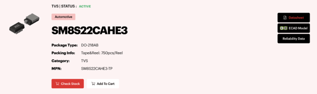
Figure 1 – SM8S22CAHE3 product page
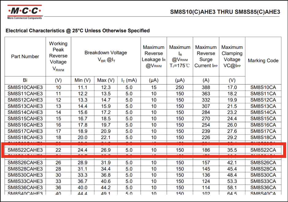
Figure 2– Datasheet of SM8S22CAHE3
To further support the TVS selection process, this application note includes both SPICE simulation results and load dump qualification test report of the selected part number. While the calculations define the minimum electrical requirements and the simulation illustrates the expected transient response, the test report demonstrates the capability of the selected TVS diode under load dump conditions that are more demanding than those used in the design calculations.
This comparison shows that the simulated operating conditions are encompassed within the tested performance of the device, providing additional confidence that the selected TVS not only satisfies the calculated ISO 16750-2 requirements but also offers additional robustness for real-world automotive applications.
03
TVS SPICE SIMULATION – ISO 16750-2: TEST A
To obtain a more accurate representation of the performance of the selected TVS for this application, a brief SPICE simulation was performed, and the results were compared with the analytical calculations. It is important to note that this comparison focuses on evaluating the accuracy of the equations used during the TVS selection process, as the device had already been selected in the initial design step and the simulation is used solely to validate its expected behavior.
.png?width=832&height=754&name=image%20(1).png)
Figure 3 – SPICE simulation results of TVS under Load Dump transient
Since the simulation uses fixed breakdown and clamping voltage values, the comparison focuses on the remaining parameters. In this case, the Load Dump generator provided by Analog Devices produces a surge voltage (VP) of 98.512V, compared to the 101V defined by ISO specifications and used in the calculations. The simulated clamping voltage (VC) is 26.697V, while the maximum value established for calculation was 35V. Similarly, the simulated peak pulse current (IPP) reaches 17.638A, compared to the calculated value of 16.5A.
For the peak pulse power (PPP), the simulation yields 470.88W, whereas the analytical calculation predicts 577.5W. Additionally, the time at which the peak pulse current (IPP) decays to 50% occurs at 84ms in the simulation, while the calculated value was 88ms. Refer to Table 1 for side-to-side comparison of these values.
Although slight deviations are observed between the SPICE simulation and analytical results, these differences are expected and remain within an acceptable range for engineering evaluation. The analytical calculations were intentionally based on conservative design parameters and worst-case conditions defined by ISO 16750-2 to support robust TVS diode selection for automotive Load Dump protection. In contrast, the SPICE simulation evaluates the behavior of the selected TVS diode under a specific load dump transient, providing a more realistic representation of its response.
It is also important to note that the analytical calculations utilize the upper limits specified by ISO 16750-2 for surge voltage (VP), pulse duration (td), and internal resistance (Ri). In the SPICE simulation, several parameters differ from these worst-case assumptions, most notably the surge voltage (VP), peak pulse current (IPP), and clamping voltage (VC). As a result, some variation between the calculated and simulated values is expected. Despite these differences, both methods demonstrate similar trends and confirm the suitability of the selected TVS diode for Load Dump protection.
|
Parameter |
Symbol |
SPICE Measurements |
Design with Simulation Values |
Calculated Theoretical Values |
Unit |
|
Surge Voltage |
VP |
98.512 |
98.512 |
101 |
V |
|
Clamping voltage |
VC |
26.697 |
26.697 |
35 |
V |
|
Internal Impedance |
Ri |
4 |
4 |
4 |
Ω |
|
Breakdown voltage |
VBR |
25.6 |
25.6 |
26.9 |
V |
|
Transient duration |
Load Dump |
400 |
400 |
400 |
ms |
|
Peak Pulse Current |
IPP |
17.638 |
17.954 |
16.5 |
A |
|
Peak Pulse Power |
PPP |
470.88 |
479.31 |
577.5 |
W |
|
Calculated Values with Measurements |
Calculated Values |
||||
|
Time constant Tau |
τ |
173.718 |
173.718 |
169 |
ms |
|
Pulse duration |
tp |
84 |
82 |
88 |
ms |
|
50% Power Margin |
- |
706.3 |
719.0 |
866.3 |
W |
Table 1 – Comparison of Analytical Calculation, SPICE Simulation, and Measured Results for ISO 16750-2 Load Dump Validation
In Table 1, both methods are set to use the same conditions. Once this is done, they are very similar to each other with a slight difference in pulse duration (tP) and peak pulse power (PPP) which concludes as acceptable results between calculation and simulation on SPICE.
04
ISO 16750-2 LOAD DUMP TEST RESULTS AND TVS VALIDATION
While calculating a TVS diode for protection of overvoltage on our circuits is a good approach, we want to ensure the reliability of the device on the real-life application, therefore the selected part number was experimentally validated by our team to confirm, beyond simulation and analytical calculations, that this TVS family is suitable for surge events such as the Load Dump. The following figures show the test conditions and resulting waveforms for the SM8S22CAHE3 TVS device under Test A conditions.
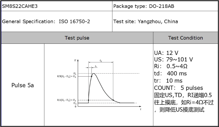
Figure 4: Test conditions for SM8S22CAHE3 TVS under Load Dump pulse
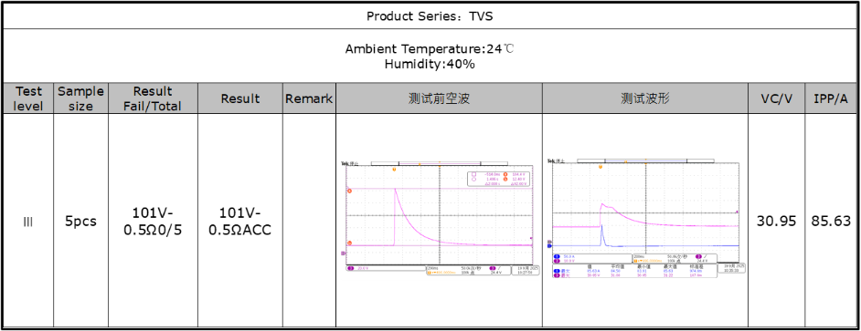
Figure 5: Test results for SM8S22CAHE3 TVS under Load Dump pulse
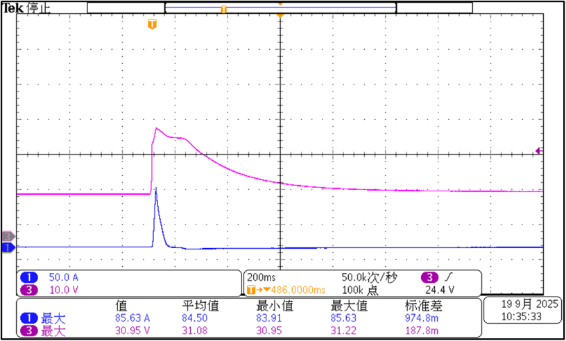
Figure 6: Current and Voltage waveform of TVS during Load Dump transient
05
CORRELATION BETWEEN ANALYTICAL CALCULATION, SPICE SIMULATION, AND LOAD DUMP TEST RESULTS
The analytical calculations presented in Part 1 establish the electrical requirements required for selecting a suitable TVS diode under ISO 16750-2 load dump conditions. By adopting conservative assumptions and worst-case design parameters, the calculations provide a robust foundation for initial device selection.
The SPICE simulation further validates the analytical methodology by reproducing the transient behavior of the selected TVS diode under the defined load dump conditions. Although small deviations exist due to differences in surge voltage, clamping voltage, and pulse characteristics, the simulation closely follows the analytical predictions and confirms the suitability of the selected device.
Finally, the ISO 16750-2 load dump qualification test report provides the highest level of validation. Unlike the analytical calculations, which are based on design requirements, the qualification test subjects the TVS diode to repeated load dump pulses under more demanding conditions. The successful completion of these tests demonstrates that the selected SM8S22CAHE3 not only satisfies the calculated requirements but also provides additional design margin for real-world automotive applications.
Together, the analytical calculations, SPICE simulation, and qualification test results establish a complete verification methodology that increases confidence in the TVS selection process while improving the robustness and long-term reliability of automotive surge protection designs.
06
Conclusions
This two-part application note presented a practical methodology for selecting and validating a TVS diode for automotive load dump protection in accordance with ISO 16750-2.
Part 1 introduced the load dump phenomenon, explained the key TVS diode selection parameters, and demonstrated a step-by-step calculation method for determining the required Reverse Working Maximum Voltage (VRWM), Breakdown Voltage (VBR), Clamping Voltage (VC), Peak Pulse Current (IPP), and Peak Pulse Power (PPP).
Part 2 extended this methodology by validating the selected TVS diode through SPICE simulation and ISO 16750-2 load dump qualification testing. The close correlation between analytical calculations, simulation, and qualification test results confirms the effectiveness of the design approach while demonstrating that the selected TVS diode provides additional design margin beyond the calculated requirements.
By combining analytical calculations, simulation, and qualification testing, engineers can develop more robust automotive surge protection solutions, reduce design risk, and accelerate product development for ECUs, battery management systems (BMS), DC-DC converters, power distribution modules, infotainment systems, and other vehicle electronic systems exposed to load dump transients.
To support a wide range of automotive surge protection requirements, MCC offers a comprehensive portfolio of AEC-Q101 qualified TVS diodes specifically designed for ISO 16750-2 load dump protection in the robust DO-218AB package. The portfolio includes the SM8S Series (6.6 kW), and SM8Z Series (8.0 kW), providing multiple power ratings to meet different automotive design requirements. Whether designing compact electronic control units or high-power automotive systems, engineers can select the most appropriate TVS solution while maintaining compliance with demanding automotive surge protection standards.
Explore the complete MCC Automotive Load Dump TVS portfolio and datasheets to find the right protection solution for your next automotive power design. To help engineers further understand transient protection, automotive reliability, and TVS diode selection, MCC has developed a comprehensive collection of technical resources covering TVS fundamentals, application design, and real-world implementation. Continue Exploring MCC's TVS Protection Knowledge Center:
- Understanding TVS Diodes: A Comprehensive Guide
- Three Fascinating Facts About TVS Diodes
- Safeguarding Sensitive Electronics: The Importance of TVS Diodes
- Application Note: Enhancing Data Center Reliability with TVS Diodes in Hot-Swap Controllers
- Made for Harsh Environments: MCC's Automotive-Grade TVS Series
07
References
- Micro Commercial Components (MCC). Understanding TVS Diodes: A Comprehensive guide. Retrieved from: https://solutions.mccsemi.com/understanding-tvs-diodes-a-comprehensive-guide
- Micro Commercial Components (MCC). (2025, May 13). Application Note: Enhancing Data Center Uptime with TVS Diodes in Hot-Swap Controllers. MCC - Application Notes. Retrieved from: https://solutions.mccsemi.com/news/hot-swap-controller-application-note-enhancing-data-center-reliability
- Analog Devices. (2019, August 19). Load-Dump Protection for 24V Automotive Applications. Technical Articles. Retrieved from:
https://www.analog.com/en/resources/technical-articles/loaddump-protection-for-24v-automotive-applications.html - Wang, Q. (2022). TVS Diode Selection and Theoretical Calculation in Automotive Electronics. Advances in Transdisciplinary Engineering, Volume 33: Mechatronics and Automation Technology, 10.3233/ATDE221218. Retrieved from:
https://doi.org/10.3233/atde221218 - International Organization for Standardization. (2011). ISO 7637-2:2011. ISO. Retrieved from: https://www.iso.org/standard/50925.html
- International Organization for Standardization. (2023). ISO 16750-2:2023. ISO. Retrieved from: https://www.iso.org/standard/76119.html
- International Organization for Standardization. (2023a). ISO 16750-1:2023. ISO. Retrieved from: https://www.iso.org/standard/77578.html
- International Organization for Standardization. (2023b). ISO 7637-1:2023. ISO. Retrieved from: https://www.iso.org/standard/83230.html
- Analog Devices. (2017, 5 April). LTspice: Models of ISO 7637-2 & ISO 16750-2 Transients (D. Eddleman, Ed.). Retrieved from:
https://www.analog.com/en/resources/technical-articles/ltspice-models-of-iso-7637-2-iso-16750-2-transients.html - Bimbhra, P. S. (1999). Power Electronics (Third Edition). Khanna Publishers.
Micro Commercial Components, Corp., (MCC)