How SBD, JBS, and MPS SiC Diodes Differ in Real Designs
SBD (Schottky Barrier Diode)

|
Structure: A single metal contact on an n-type SiC wafer. Key Physics: Majority-carrier conduction through the metal–semiconductor barrier, resulting in extremely fast switching and negligible stored charge. |
Strengths:
- Ultra-fast switching with minimal reverse recovery
- Lowest intrinsic switching loss for a given voltage class
- Simple fabrication with fewer masks and implants
Weaknesses:
- Higher reverse leakage, especially at elevated temperatures
- Reduced tolerance to high electric-field stress and transient overloads
Typical Metrics:
- Forward voltage (Vf) vs. current and temperature
- Reverse leakage (IR) vs. reverse voltage and temperature
- Surge current capability (IFSM)
Best For: High-frequency converters, PFC stages, and DC-DC converters with limited surge exposure.
JBS (Junction Barrier Schottky)

|
Structure: Schottky metal contact with small p-type (often p+) islands implanted beneath the metal, interleaving PN regions with Schottky areas. Key Physics: Under reverse bias, p islands form PN junctions that shift peak electric fields away from the metal interface, reducing leakage and improving breakdown stability. Under forward bias, current flows mainly through Schottky regions. |
Strengths:
- Much lower reverse leakage than SBD
- Improved breakdown stability and transient robustness
- Maintains near-Schottky switching speed
Weaknesses:
- Moderate surge handling (better than SBD but without conductivity modulation)
- More complex processing due to ion implantation and extra masks
Typical Metrics:
- Reverse leakage (IR) at rated voltage across temperature
- Forward voltage (Vf) at operating current and temperature
- Surge current (IFSM) and UIS robustness
Best For: High-voltage applications where leakage control and stable blocking matter, including server and telecom power supplies, onboard chargers, and grid converters.
MPS (Merged PiN Schottky)

|
Structure: Interleaved Schottky fingers and larger, heavily doped p+ regions forming local PiN segments merged with Schottky areas. PiN conduction activates only during high-current events. Key Physics:
|
Strengths:
- Excellent surge current capability and thermal ruggedness
- Very low reverse leakage due to strong electric-field shielding
- Combines low normal-operation loss with high transient robustness
Weaknesses:
- Slight increase in reverse recovery when PiN regions activate during surge (still far lower than silicon PiN diodes)
- Requires precise implant control and thin-wafer processing
Typical Metrics:
- Forward voltage (Vf) vs. current and temperature
- Reverse leakage (IR) vs. reverse voltage across temperature
- Surge current (IFSM), UIS, and transient stress tests
- Reverse recovery (Qrr) if PiN conduction may occur during switching
Best For: EV chargers, PV inverters, energy-storage systems, and automotive power electronics.
JBS vs MPS: Quick Technical Comparison
|
Category |
JBS (Junction Barrier Schottky) |
MPS (Merged PiN Schottky) |
|
|
|
|
|
Structure |
Combines Schottky metal contact with embedded p+ guard regions beneath the metal |
Similar to JBS, but with periodically merged p+ PiN regions forming hybrid conduction paths |
|
Current Flow |
Primarily through the Schottky region under forward bias |
At low current → Schottky conduction; at high current → additional PiN conductio |
|
Forward Voltage (Vf) |
Lower (since current mainly flows through Schottky contact) |
Slightly higher (due to contribution from PiN regions at high current) |
|
Reverse Leakage Current |
Low |
Very low (enhanced shielding from p+ regions) |
|
Surge Current Capability |
Moderate |
Excellent: PiN regions conduct under surge or high-temperature stress |
|
Thermal Ruggedness |
Moderate |
High: improved high-temperature and avalanche performance |
|
Reverse Recovery |
Very fast (pure Schottky behavior) |
Fast, but slightly slower than pure Schottky due to minority carrier injection in PiN regions |
|
Reliability |
Good: stable leakage characteristics |
Better: higher reliability margin and robustness under stress. |
|
Application Focus |
Efficiency-oriented applications |
Ruggedness and reliability-oriented applications |
|
Typical Applications |
Server/Telecom PSU, DC-DC converters (light load), OBC |
EV chargers, PV inverters, industrial power supplies |
|
Summary |
Optimized for low Vf and high efficiency |
Optimized for high surge, thermal robustness, and reliability |


How to Choose the Right MCC SiC Schottky Generation
The tables above show how MCC’s SiC Schottky technology has evolved across generations. The next step is translating those differences into a practical selection decision based on real operating conditions.
Rather than optimizing a single parameter, each MCC generation is intentionally designed to balance efficiency, robustness, and cost for different application priorities. The right choice depends on where your design sits in terms of temperature, switching behavior, surge exposure, and system cost targets.
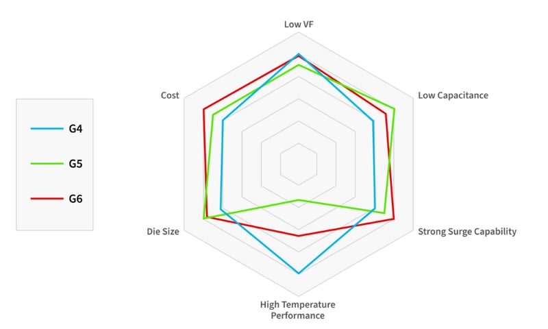
Figure 1: Illustration comparing three MCC SiC Schottky technology generations (G4, G5, and G6)
This illustration provides a visual summary of the relative trade-offs across key design considerations, including forward voltage (Vf), junction capacitance (Cj), surge current capability (IFSM), high-temperature performance, die size, and cost. It does not represent absolute values; instead, it highlights how each generation is optimized in different areas to support specific use cases.
Practical Guidance by Generation
G4: Thermal Stability and Proven Performance
G4 devices are optimized for strong high-temperature performance and stable operation. They are well suited for designs that operate continuously at elevated junction temperatures or where thermal margin, and long-term reliability are primary concerns.
Typical applications include:
-
On-board chargers (OBC)
-
Energy storage inverters
-
Residential and commercial inverter systems
G5: Switching Performance and Efficiency Balance
G5 focuses on lower capacitance and improved switching behavior, while maintaining solid surge capability. This makes it a strong choice for higher-frequency power conversion designs where switching loss and overall efficiency directly impact system performance.
Typical applications include:
- EV chargers
- Grid-tied PV inverters
- High-efficiency power conversion stages
G6: Surge Robustness and Cost Optimization
G6 emphasizes strong surge current capability and cost efficiency, enabled by process and die-size optimization. It is designed for applications exposed to frequent transients or surge stress, where value optimization is important without sacrificing core electrical performance.
Typical applications include:
- EV chargers with high surge exposure
- Micro inverters
- Cost-sensitive industrial power supplies
A Generation-Based Selection Framework
Instead of asking “Which SiC Schottky is best?”, a more practical question is:
“Which generation best matches my operating conditions?”
A generation-based approach allows designers to:
- Match device performance to real system stress
- Avoid unnecessary over-design
- Optimize efficiency, reliability, and cost at the system level